


Next: 3.4 Process Simulation
Up: 3. The TCAD Concept
Previous: 3.2 Overview
Subsections
To start with the process simulation block some information has to be
prepared in a certain level of detail.
As in real semiconductor processing the layout of the device or integrated
circuit is a substantial input to the fabrication flow. It defines the lateral
composition of the circuitry and is the main variable input to the
semiconductor fabrication line 3.1. The
layout consists of the combination of a set of different mask levels. Each
mask level is defining a certain functional block during processing. As one
example, the gate level defines the sizes and orientation
of any CMOS gate inside the integrated circuit. As another example, the Boron
source/drain masks define the areas where the Boron for the PMOS source/drain
regions has to be implanted. The combination of these mask levels
characterizes the overall structure of certain devices. A simple example of
this concept is shown in Figure 3.3.
Figure 3.3:
Simple layout example of a PMOS transistor
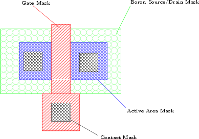 |
It can be seen from this figure that the source/drain implant is drawn over
the gate layer too. However since in the fabrication process the gate layer is
masking the implantation, the real source/drain diffusion is only the logical
NOR operation of the two layers.
3.3.2 Mask Bias
Mask bias is a post processing step during the fabrication of the chrome
reticle masks for lithography. Especial the patterning process is subject to
process related variations which have to be compensated with lithography. A
good example is the somewhat outdated 3.2 process module LOCOS (LoCal Oxidation of Silicon) [120]
isolation. Figure 3.4 shows the detailed process step chain
of this module.
Figure 3.4:
Typical LOCOS module sequence
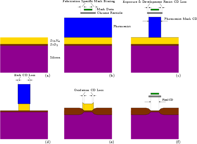 |
Figure 3.4(a) shows the initial stack of the LOCOS sequence
consisting of the single crystalline silicon substrate, the so called pad
oxide consisting of Silicon Dioxide as a stress relief layer and Silicon
Nitride which acts as oxidation suppression mask for the oxidation of
silicon. Figure 3.4(b) shows the situation after spin-on of
the photo resist. On top of the structure the chrome reticle dimension for the
subsequent illumination step is shown. Furthermore, the initial dimension of
the mask data is shown. Since the drawn layout dimension should define the
final size of the area of the active region (the region not covered by field
oxide), the real chrome area has to be bigger (biased) in
size. A detailed outline of the algorithm for proper biasing of the
two-dimensional layout structures is given in Appendix C.
Figure 3.4(c) shows the situation after illumination,
development and hard bake of the photo resist. A couple of effects, like under
or overexposure, resist shrink during post exposure bake etc., may lead to
differences in the width of the photo resist structure and the initial reticle
dimension. These differences are the first contribution to the CD (critical
dimension) difference between the initial reticle size and the final size of
the structure of silicon. Figure 3.4(d) shows the CD loss
because of a small undercut of the Silicon Nitride during layer
etch. Additional CD loss may occur if the etching chemistry consumes small
parts of the capping photo resist layer. Figure 3.4(e) shows
the CD loss due to encroachment of the silicon nitride capping layer during
oxidation of the silicon. Finally Figure 3.4(f) gives the
situation after stripping of the capping nitride layer. If the initial
reticle mask bias compensates for the above mentioned effects during the
steps (c) through (e) in Figure 3.4, the final CD matches exactly the initially drawn layout
dimension. Since the processing effects depend critically on the details of
the manufacturing process, this biasing is called fabrication specific.
Another important convolution of the initial mask input to process simulation
are the mask proximity effects due to the diffraction effects during
photo resist exposure. The underlying physics was described in
Section 2.4 in detail. A simulation taking into
account these effects is outlined in
Section 6.3. An example of the magnitude of these
effects for a typical 350nm node mask illuminated with i-line lithography is
shown in Figure 3.5.
Figure 3.5:
Initial layout of a part of an EEPROM cell (a),
contour plots of intensity distribution during the illumination
of photo resist at different levels (b)-(e) and resulting resist
contours after development (f).
|
![\includegraphics[width=0.8\textwidth]{figures/eearray_layout.ps}](img135.png)
(a)
|
![\includegraphics[width=0.8\textwidth]{figures/eearray_FG.ps}](img136.png)
(b)
|
![\includegraphics[width=0.8\textwidth]{figures/eearray_P1.ps}](img137.png)
(c)
|
![\includegraphics[width=0.8\textwidth]{figures/eearray_CO.ps}](img138.png)
(d)
|
![\includegraphics[width=0.8\textwidth]{figures/eearray_M1.ps}](img139.png)
(e)
|
![\includegraphics[width=0.8\textwidth]{figures/eearray_contours.ps}](img140.png)
(f)
|
|
Figure 3.5(a) shows the initial layer data for some
levels during fabrication of a EEPROM cell [11],[122] (Floating Gate, Gate Poly, Contact
and Metal 1). Figure 3.5(b) through
Figure 3.5(e) show the intensity distribution during resist
illumination. Figure 3.5(f) shows the extracted iso
contours (at same level of intensity) of the 4 layers demonstrating the above
mentioned proximity effects during lithography.
By applying these simulations the resulting proximity corrected contours can be
used as an input to the process simulation in the usual CIF or GDSII
formats. Therefore, the layout may be preprocessed once to reflect the real
mask shapes more closely. To simplify the resulting contour polygons a
polygon point reduction algorithm, the minmax-method [123]
has been used. An example of the results of such a preprocessing of
the mask layout can be found in Section 6.3
In Chapter 2 it has been outlined, that
the clean room production flow is a fairly linear flow but of high
complexity with respect to the production path in the
fabrication. Since this flow has to be documented extremely well to
prevent misprocessing, a so called MES (Manufacturing Execution
System) is used to control the wafers during their full processing
flow. Controlling means tracking of the current position in the
process flow and defining the correct machine recipes at the correct
positions of the flow. This process flow (to name it short) is a list
of single process steps which determine WHEN and HOW the wafer surface
has to be modified by implantation, etching, deposition, and masking to
form an integrated circuit at the end.
There are two classes of process simulation steps. On one side the
``physical'' process steps ion implantation, oxidation and diffusion
where the machine parameters (recipes) are inputs to the process
simulation also. In contrast to this class there are the ``chemical''
process steps etching and deposition, where currently there are no
stable, reliable and sufficiently fast models available to model these
steps with their process recipes (pressure, temperature over time)
rigorously. These steps are modeled via simple geometric ``emulation''
of the outcoming topology change after the run recipe. Therefore, the
calibration of these steps is very important. Lithography is in part
``physical'' (illumination) and in part ``chemical'' (PAC reaction and
development), and normally it its treated as deposition and
etching in terms of geometrical modeling. In terms of illumination it
has been shown in the previous section, how to care about these effects.
To finally get the deserved simulation results by process
simulation with appropriate accuracy, it is mandatory to
mimic the real processing with a high level of detail provided
by the physical models of the process simulator. A good example of
such an approach is the implementation of a diffusion and oxidation
recipe in a process simulator as shown in
Section 6.1. In this example every
single change in temperature (temperature ramps) or pressure (pressure
ramps) or gas ambient change (oxidizing ambient instead of inert
ambient) above a certain temperature where the diffusion models of
the process simulator are calibrated and valid, was defined as a
single command for the process simulator. The final simulation program
consists of a sequence of different process conditions of a certain
time. In the past this concept was not employed because of the big
penalty in simulation time. In contrast only the ``main thermal step''
was defined as a process simulation command. The new concept has the
big advantage of being not prone to the judgement of the TCAD engineer,
which of the numerous single diffusion steps (between 8 and 30) is now
the most dominant and important one.
In Table 3.1 a comparison of the
current levels of details in the process flow information according to
the current status of the physical models of the available process
simulators is given. The process steps deposition, etching, and
lithography were left out on purpose since these steps are normally
not modeled via equipment level simulation (input parameters to the
simulation are the process recipes) but via geometrical approximation
as outlined above.
Table 3.1:
Examples for
current level of details in the description of semiconductor process steps
| Step |
Low Detail |
Medium Detail |
High Detail |
|---|
| diffusion |
temp. |
pressure |
temp. |
pressure |
temp. |
pressure |
| & |
time |
flow rates |
time |
flow rates |
time |
flow rates |
| oxidation |
|
|
temp. ramps |
|
temp. ramps |
gas ramps |
| |
of main diff. step |
of all diffusion steps |
of all diffusion steps |
| ion |
dose |
energy |
dose |
energy |
dose |
energy |
| implantation |
tilt |
|
tilt |
revolving |
tilt |
revolving |
| |
|
|
|
|
beam div. |
ioniz. level |
|
Footnotes
- ... line 3.1
- except the process technology itself which
could be varied based on the needs of the product, however in a standard
semiconductor fabrication the number of different process technologies is far
less than the number of integrated circuits on ONE technology platform
- ... outdated 3.2
- the module is the standard
approach for the transistor isolation for technology nodes
 250nm
250nm
Next: 3.4 Process Simulation
Up: 3. The TCAD Concept
Previous: 3.2 Overview
R. Minixhofer: Integrating Technology Simulation
into the Semiconductor Manufacturing Environment