Line-edge roughness plays an important role on the characteristics of narrow GNRs. Experimental data show that line-edge roughness is the dominant scattering mechanism for GNRs narrower than 60nm [180]. Line-edge roughness causes fluctuations in the edge potential and leads to the modulation of the energy gaps which affects optical transitions and photon absorption energies. Therefore, a careful investigation of this effect on the optical properties of GNR superlattices is essential. Line-edge roughness is a statistical phenomenon that can be well described by means of an exponential autocorrelation function [179]:
|
| (5.1) |
where ΔL is the roughness correlation length which is a measure of smoothness and ΔW is the root mean square of the fluctuation amplitude. To create line-edge roughness in real space, a random phase is added to the Fourier transform of the autocorrelation function (power spectrum) followed by an inverse Fourier transform [181]. Using the obtained roughness profiles various devices are generated. The optical characteristics of each device is evaluated separately, followed by an ensemble average.
The effect of line-edge roughness on the electronic properties of GNRs has been investigated in several analytical [179,182] and numerical studies [183,184]. Here, we investigate the role of roughness on the spectrum of photocurrent in GNR-based superlattices.
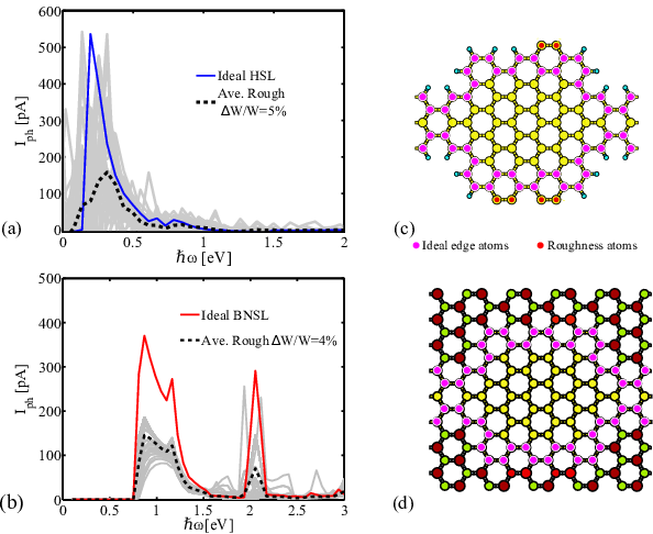
We add/remove an integer number of atoms from the edges based on their relative position with respect to the generated rough edge. However, this may result in an unstable edge-structures with monomers instead of dimers at the edges. In these cases, the edges are reconstructed to be physically stable. For the given geometrical and roughness parameters many samples are statistically generated. The characteristics of each device is evaluated followed by an ensemble average over all samples, see Fig. 5.7. More details about our approach can be found in [181].
Due to backscattering of carriers, the photocurrent and quantum efficiencies of both supper lattices decrease in the presence of line-edge roughness. Figure 5.7 shows that due to effective width variation, the photoabsorption peaks appear at energies larger or smaller than the peaks of the structure without disorder. The average width of edge-defected devices, however, is equal to that of a device with perfect edges. Therefore, line-edge roughness does not affect the location of the average photocurrent peak.
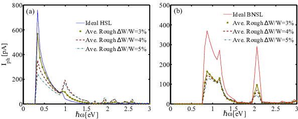
Figure 5.8 exhibits the results for HSL(11) and BNSL(11) with edge disorders. Roughness is expressed in terms of nw because the well has a more significant effect on the optical transitions. The absolute roughness amplitude is the same all over the device. In the case of BNSL(11), the roughness is applied at the C-BN interfaces. As it is shown in Fig. 5.1, a BN passivation with 2/3 dimers is considered in BNSLs. For the roughness amplitudes of 3%, 4%, and 5%, the structures are still passivated with BN. However, for larger roughness amplitudes the roughness may cross the boundaries without any BN passivation. In these cases, the structures are reconstructed by additional BN dimmers at the boundaries.
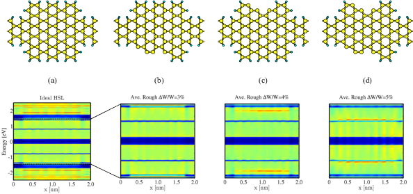
HSL(11) exhibits photoresponsivity and quantum efficiency reductions of 23%, 55%, and 70% for the relative roughness amplitudes of 3%, 4%, and 5%, respectively, whereas a smoother behavior is observed for BNSL(11) (compare Fig. 5.8(a) and (b)). This behavior is attributed to the stable configuration of edge-carbon atoms in BNSL in comparison with HSL in the presence of line-edge roughness. The average photocurrent of edge-defected HSLs peaks at photon energies around ℏω = 1eV. This peak is related to line-edge roughness induced states, see Fig. 5.9. Due to the formation of dangling bonds in the presence of line-edge roughness, these states are formed. As the relative roughness amplitude increases more states are induced and more photocurrent is generated by transitions from these states. However, dangling bonds are absent in edge-defected BNSLs and such states do not appear in such structures.