5.1 Graphene Superlattice Properties
Table 5.1: The proposed TB model parameters for the superlattice. All
parameters are expressed in electron volt.
|
|
|
|
|
|
|
|
|
|
|
|
| tCC | tBB | tNN | tBC | tNC | tBN |
|
|
|
|
|
|
| 2.35 | 0 | 0.45 | 2.1 | 2.4 | 2.8 |
|
|
|
|
|
|
|
|
|
|
|
|
| tCC,2 | tBC,2 | tNC,2 | △CC | △BB | △NN |
|
|
|
|
|
|
| 0 | 0.1 | 0.3 | 0.015 | 2.05 | -2.05 |
|
|
|
|
|
|
| | | | | | |
| |
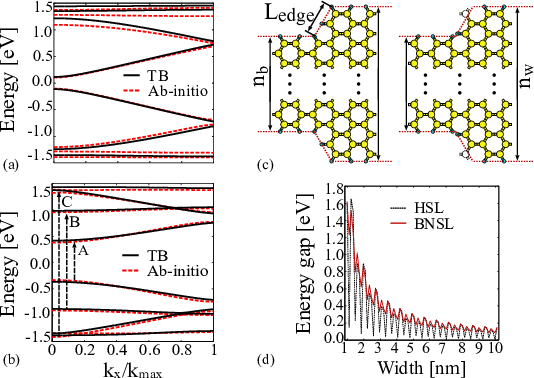
Figure 5.2 compares the bandstructures for HSL(11) and BNSL(11) based on
the TB model and first principles calculations. Carbon-carbon interactions up to
three nearest neighbors are considered in the TB calculations for HSLs. In the
case of BNSLs, a more careful choice of the TB parameters is required
due to the ionicities of the boron and nitrogen atoms at the edges of the
superlattice. The tight-binding parameters proposed in Table 5.1 result in
electronic disperse relations that are in excellent agreement with first-principle
simulations. In this table, tXY and tXY,2 denote the hopping parameter between
the first and second nearest neighbor X and Y atoms, where X and Y
represent carbon C, boron B, or nitrogen N atoms. ΔXX denotes the on-site
potential of atom X. As shown in Fig. 5.2(a), larger energy gaps are achieved
for BNSLs in comparison with HSLs, which is attributed to the large
ionic potential difference between boron and nitrogen atoms in BNSLs
[135].
The bandgap as a function of the width of superlattice is depicted in
Fig. 5.2(d). Zigzag edges in a graphene layer induce an opposite spin orientation
across the ribbon between ferromagnetically ordered edge state [178]. In such
cases, additional spin analysis is necessary which is beyond the scope of this work.
To avoid zigzag edges, we assumed that nw and nb are scaled such that
Ledge is kept constant, where nw and nb are defined as the number of
dimer lines in the well and barrier of the superlattice, respectively, see
Fig. 5.2(c). Figure 5.2(d) shows that HSLs, unlike BNSLs, have relatively small
bandgap for specific values of nw = 3p + 2, where p is a positive integer. In
addition, the scaling of the energy gap with the width in BNSLs shows a
more uniform behavior compared to that of HSLs. An important point
to notice is the instability of the superlattice shown in the right side of
Fig. 5.2(c) as a result of the dangling bonds, which will quickly relax
to form another geometry. In fact, all superlattices with even values of
nw are unphysical, and thus the studies are restricted to odd values of
nw.
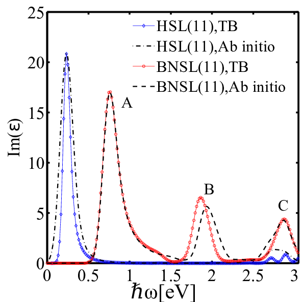
The optical response of the superlattices presented in Fig. 5.1 is studied in
terms of the interband dielectric response function (Eq.3.4). The details of
dielectric response function is presented in Sec. 3.1.1.
Figure 5.3 compares the imaginary parts of the dielectric functions for a
HSL(11) and a BNSL(11). The absorption spectrum exhibits its first peak at
ℏω = 0.33eV which corresponds to a transition from the highest valence band to
the lowest conduction band. The optical absorption spectrum of BNSL(11)
exhibits additional peaks in the photon energy range 0 < ℏω < 3.5eV. The
absorption peaks occur at the photon energies of 0.91eV, 1.965eV, and
3.156eV which are related to transitions represented by A, B, and C in
Fig. 5.2(b), respectively. The comparison of the dielectric functions in
Fig. 5.3 with the bandstructures shown in Figs. 5.2(a) and (b) suggests
that for this specific structure only transitions from valence bands to
conduction bands with the same index are allowed. This, however, is not a
general transition rule for BNSLs and does not hold at various geometrical
parameters.
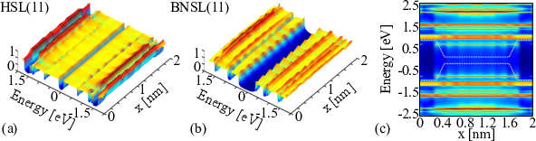
In order to get a deeper understanding on the operation of such structures the
local density of states (LDOS) and photocurrent need to be carefully considered.
Figures 5.4(a) and 5.4(b) show the LDOS for the superlattices under study. These
LDOS plots indicate the presence of localized states in both structures. The
normalized LDOS for the unit cell of an ultrathin HSL is shown in Fig. 5.4(c).
It is predictable that the first peak in the optical spectrum occurs at
ℏω = 1.5eV which is related to an optical transition between the two
confined states at energies 0.74eV and 0.69eV (See Fig. 5.4(c)). Since the
presence of these two states is forbidden in the barrier regions of the
superlattice, the photocurrent at ℏω = 1.5eV is completely of quantum
mechanical nature. At higher energies some continuous minibands are
formed which give rise to the photocurrent observed at approximately
ℏω = 2eV.
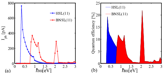
In order to assess the performance of superlatice structures for photodetection
applications, the quantum efficiency and the photoresponsivity of the
presented structures are evaluated. The quantum efficiency is defined as
α =  ∕
∕ , where Iph and Pop are the photocurrent and the incident
optical power, respectively. Figure 5.5(a) and (b) shows the calculated
photocurrent and quantum efficiency as a function of the incident photon
energy, respectively, for HSL(11) and BNSL(11). The quantum efficiency
peaks if the photon energy corresponds to an allowed intersubband optical
transition. The quantum efficiency of the HSL reaches the values of about 20%,
which is significantly larger than that of H-AGNRs [171]. For the case of
BNSL(11), there are more peaks in the specified energy range due to the
different subband spacings in comparison with that of HSL(11). Quantum
efficiencies of 13% and larger than 20% are obtained for the first and
second peaks in the optical spectrum, respectively. The photoresponsivities-
defined as Iph∕Pop- of HSL and BNSL reach 0.866A∕W and 0.303A∕W,
respectively, where the optical power is assumed to be 100 kW∕cm2.
, where Iph and Pop are the photocurrent and the incident
optical power, respectively. Figure 5.5(a) and (b) shows the calculated
photocurrent and quantum efficiency as a function of the incident photon
energy, respectively, for HSL(11) and BNSL(11). The quantum efficiency
peaks if the photon energy corresponds to an allowed intersubband optical
transition. The quantum efficiency of the HSL reaches the values of about 20%,
which is significantly larger than that of H-AGNRs [171]. For the case of
BNSL(11), there are more peaks in the specified energy range due to the
different subband spacings in comparison with that of HSL(11). Quantum
efficiencies of 13% and larger than 20% are obtained for the first and
second peaks in the optical spectrum, respectively. The photoresponsivities-
defined as Iph∕Pop- of HSL and BNSL reach 0.866A∕W and 0.303A∕W,
respectively, where the optical power is assumed to be 100 kW∕cm2.
In this study, a small voltage bias in the range of 0.05-0.1V is applied to drive
the generated electrons and holes towards the contacts. The restriction for the
applied voltage bias is the band to band tunneling which increases the dark
current and is detrimental for photodetectors. The tunneling current has an
exponential dependence on the electric field. Due to the relatively small length of
proposed superlattice photodetectors, applying even a small voltage bias may
cause a huge electric field. For example a voltage bias of 0.1V leads to an electric
field of 4.7 × 10⁵V/cm.
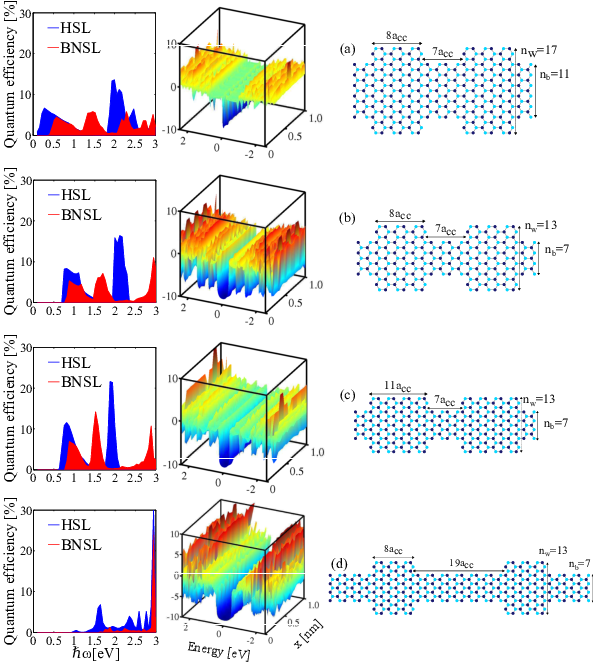
The structural parameters effects on superlattice photodetector characteristics
are examined. Figures 5.6(a) and 5.6(b) indicate that more peaks appear in the
quantum efficiencies of HSL/BNSL(13) and HSL/BNSL(17) compared to the
main structure (Fig.5.5(b)). If the width of the superlattice increases, energy gaps
decrease which allow more optical transitions. This behavior is similar to that of
GNRs [179], however, in superlattice photodetectors, the quantum efficiencies at
higher energies are larger in comparison with that of lower energies. This is
due to the presence of barriers that block transport of photo-generated
carriers which is more pronounced by increasing the barrier/well lengths, see
Fig. 5.6(c) and Fig. 5.6(d). It should be noted that the confinement due to the
presence of barriers only weakly affects devices with relatively long wells
and the characteristics of such structures become similar to conventional
GNR-photodetectors.