|
|
|
|
Dissertation Martin Wagner | Previous: 6. Case Studies Up: 6. Case Studies Next: 6.2 Non-Ideal Devices and Thermal Environment |
|
|
|
|
Dissertation Martin Wagner | Previous: 6. Case Studies Up: 6. Case Studies Next: 6.2 Non-Ideal Devices and Thermal Environment |
The first type of thermoelectric generators, which is also the one usually used in commercial energy conversion applications, has inherited its principle assembly from early thermocouples and temperature sensors. It consists of two semiconducting legs, where one is made of p-type and the other of n-type material. In practical devices, the p-type leg is designed with a larger cross section than the n-type one due to the lower hole mobility. While the two legs are thermally parallel, they are electrically connected in series by a contact at the heated end of the devices. Due to the different signs of Seebeck coefficients in differently doped materials, the total voltage of the device is the sum of the single contributions of each leg.
In practical applications, thermoelectric modules are constructed of several single thermoelements, as sketched in Fig. 6.1. There, a possibility to adapt to thermal and electrical specifications is the different connection of single elements to modules in both an electrical as well as a thermal sense. While electrically parallel connection of single elements increases the total current, a serial configuration is applied to enhance the output voltage. The same principle works for the thermal configuration. Multiple single elements on the same level increase the heat flux throughout the entire module in order to exploit relatively "strong" temperature reservoirs at temperature differences matching one single stage. Environments with higher temperature differences are often treated with modules consisting of multiple stages. There, the temperature difference is subdivided to a thermally serial configuration within stacked modules. Since every material has an ideal thermal operating point, as outlined in Chapter 4, it is often beneficial to combine stages built of different semiconductors.
In the sequel, the basic behavior of single thermoelements is discussed on the basis of simulation results. In order to analyze the internal behavior of a single thermoelectric device, the focus is put on the thermoelectrically active device itself first. In this idealized perspective of thermoelectric generators, thermal contact resistances as well as characteristics of heat sources and sinks are neglected. This means that the thermoelectrically active legs capitalize from the entire thermal potential, which is provided by ideally stiff temperature sources. Furthermore, electric contact resistances are neglected as well. Such a treatment is beneficial in order to identify the maximum conversion potential of a thermoelectric device, which will be reduced by parasitic external effects in practical situations. Furthermore, it enables an analysis of the internal mechanisms, which governs valuable insights for device optimization and further development.
In Fig. 6.2, the current and voltage behavior of a single
thermocouple with respect to a load resistance is illustrated for different
temperature differences. The device assumed has a leg length of
![]() and a cross section of
and a cross section of
![]() . Both legs are made of silicon
and have according doping concentrations of
. Both legs are made of silicon
and have according doping concentrations of
![]() .
The electric contacts are considered as ideal conductors, which is a safe
assumption for conventional device geometries. For example copper features an
electrical conductivity of
.
The electric contacts are considered as ideal conductors, which is a safe
assumption for conventional device geometries. For example copper features an
electrical conductivity of
![]() , which is about three
orders of magnitude above the conductivity of accordingly doped silicon.
, which is about three
orders of magnitude above the conductivity of accordingly doped silicon.
With a constant temperature difference maintained along the device, a simulated ohmic load resistance is swept over four decades. For low resistances, the behavior converges against short circuit conditions. While the voltage drops to zero, an accordingly high current is driven by the temperature gradient. For accordingly high resistances, the driven current goes to zero, while the voltage approaches its open circuit value. Within considerable ranges, both current and voltage increase with increasing temperature differences. This behavior is limited by strongly decreasing Seebeck coefficients at high temperatures, as presented in Figures 3.7 and 3.8.
The electrical power output is obtained as the product of contact voltage
![]() and driven current
and driven current ![]() , where the contact voltage can be obtained
as the directed integral along both legs as
, where the contact voltage can be obtained
as the directed integral along both legs as
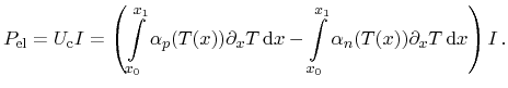 |
(6.1) |
![\includegraphics[width=10cm]{figures/simulation/power_eff.eps}](img881.png) |
The thermoelectric conversion efficiency is defined by the energy balance within the device as the ratio of generated electrical power and incoming heat-flux throughout the heated thermal contact
 |
(6.2) |
Within the idealized treatment of thermoelectric devices, the same considerations are valid for changes of the leg length, as long as the temperature at the thermal contacts can be assumed to be constant. However, in real world devices, especially in miniaturized elements, this is not the case due to the influence of parasitic external thermal resistances, as demonstrated later on. Since geometrical modifications affect both the thermal as well as the electrical circuit, the conversion efficiency and power density are not affected over a wide range. Mathematically speaking, a principle approach to performance improvement is to change the parameters of only one of the electrical and thermal subsystems as well as their coupling mechanisms. For the thermal part, it is beneficial to reduce the heat flux as much as possible while not affecting the electric conductivity. For the electric part, for example modification of the doping concentrations results in a change of the electrical conductivity. However, the Seebeck coefficient is affected reversely and thus, an optimum doping concentration can be identified.
![\includegraphics[width=10cm]{figures/simulation/doping.eps}](img884.png) |
Figures 6.4 and 6.5 point out the influence of different
doping concentrations on the device performance. The contact voltage decreases
with increasing doping due to the detrimental effect of large carrier
concentrations on the Seebeck coefficient. For comparison, see also
Figures 3.7 and 3.8. The current follows driving
voltage and internal resistance. While the driving voltage is reduced at
higher doping concentrations, the conductivity is noticeably increased. This
results in an increased current as well, as presented in Fig. 6.4.
For the power output, a trade-off between the doping's influences on current
and voltage occurs. Thus, an optimum carrier concentration exists, which is
about
![]() in the presented example. Since the carrier
contribution to the thermal conductivity is only of subsidiary significance,
the heat flux throughout the device is only increased at very high carrier
concentrations. This results in an optimum efficiency at a doping
concentration close to the one for the optimum power output.
Fig. 6.6 illustrates the temperature dependence of the electric
power output. The strongly increasing power output saturates at high
temperatures depending on the doping concentration.
in the presented example. Since the carrier
contribution to the thermal conductivity is only of subsidiary significance,
the heat flux throughout the device is only increased at very high carrier
concentrations. This results in an optimum efficiency at a doping
concentration close to the one for the optimum power output.
Fig. 6.6 illustrates the temperature dependence of the electric
power output. The strongly increasing power output saturates at high
temperatures depending on the doping concentration.
![\includegraphics[width=10.5cm]{figures/simulation/doping_eff.eps}](img886.png) |
|
|
|
|
Previous: 6. Case Studies Up: 6. Case Studies Next: 6.2 Non-Ideal Devices and Thermal Environment |
![\includegraphics[width=10cm]{figures/simulation/sketch_class.eps}](img871.png)
![\includegraphics[width=10cm]{figures/simulation/voltcurr.eps}](img872.png)
![\includegraphics[width=10cm]{figures/simulation/power_temp.eps}](img887.png)