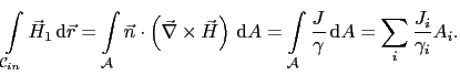
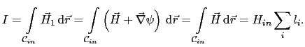
The quasi-magnetostatic case from Section 5.2 is well suited for extraction of inductance and resistance of a given structure. Distributed phenomena like proximity and skin effect can also be analyzed. The finite element method on unstructured meshes allows to obtain these parameters in arbitrary regions with complex shape, for which no analytical procedures exist. This section handles intentionally a coaxial structure, for which analytical solutions for the inductance and for the resistance exist. It is interesting to obtain these parameters numerically and compare the results with the analytical calculations, or to evaluate the method from Section 5.2 at least for this special case.
The simulated coaxial structure is shown in Fig. <6.1>. The radius ![]() of
the inner conductor is
of
the inner conductor is ![]() . The outer conductor has an inner radius
. The outer conductor has an inner radius ![]() and an outer radius
and an outer radius ![]() .
The conductor is assumed with
.
The conductor is assumed with ![]() and
and
![]()
![]() . The dielectric
material between the inner and the outer conductor (
. The dielectric
material between the inner and the outer conductor (![]() ) and outside the outer conductor (
) and outside the outer conductor (![]() )
has
)
has ![]() and
and
![]()
![]() . On the curve
. On the curve
![]() around the
inner conductor the magnetic field
around the
inner conductor the magnetic field ![]() is applied. This is managed by
applying
is applied. This is managed by
applying
![]() to each edge which belongs to
to each edge which belongs to
![]() and causes a current
and causes a current ![]() in the inner inductor
in the inner inductor
In (6.1) ![]() is the length of the
is the length of the ![]() -th edge, which belongs to
-th edge, which belongs to
![]() and the sum applies to all edge lengths building
and the sum applies to all edge lengths building
![]() .
Along
.
Along
![]() (Fig. <6.1>) the magnetic
field
(Fig. <6.1>) the magnetic
field ![]() is set consistently to zero. This requires that the current
is set consistently to zero. This requires that the current ![]() in the inner
conductor given by
in the inner
conductor given by ![]() on
on
![]() flows back in the outer conductor. The resulting
current density distribution is shown in Fig. <6.2> by directed cones placed
in the nodes of the simulation domain. The size and the darkness of the cones correspond
to the magnitude of the current density. Note that the current density in the inner conductor is not equal to the
one in the outer one, because of the different cross sections of the conductors. The corresponding
magnetic field distribution is similarly illustrated in Fig. <6.3>.
It is not difficult to see that the curves
flows back in the outer conductor. The resulting
current density distribution is shown in Fig. <6.2> by directed cones placed
in the nodes of the simulation domain. The size and the darkness of the cones correspond
to the magnitude of the current density. Note that the current density in the inner conductor is not equal to the
one in the outer one, because of the different cross sections of the conductors. The corresponding
magnetic field distribution is similarly illustrated in Fig. <6.3>.
It is not difficult to see that the curves
![]() and
and
![]() represent
the Dirichlet boundary for
represent
the Dirichlet boundary for ![]() .
The magnetic field on the edges which belong to
.
The magnetic field on the edges which belong to
![]() is
is ![]() and
zero on
and
zero on
![]() , respectively. For the
, respectively. For the ![]() field it is sufficient
that a value of
field it is sufficient
that a value of ![]() is given on one node of the simulation domain.
Since the gradient of
is given on one node of the simulation domain.
Since the gradient of ![]() is determining and not
is determining and not ![]() itself,
this value can be chosen arbitrarily.
itself,
this value can be chosen arbitrarily.
Such a coaxial structure
is well suited for the comparison between simulation and analytical results,
because analytical formulas can be given. Just homogeneous Neumann boundary
conditions (5.30) and
(5.32) are exactly satisfied also for finite
dimensions (Refer to
Fig. <6.3>). The field ![]() has no normal component to the outer
surface of the simulation domain. For isotropic materials in terms of the relative
permeability
has no normal component to the outer
surface of the simulation domain. For isotropic materials in terms of the relative
permeability ![]() the magnetic flux
the magnetic flux ![]() will have the same direction as
will have the same direction as ![]() and the Neumann boundary condition (5.30) is
satisfied independently of the size of the simulation domain. Analogously the
same can
be considered for the electric field
and the Neumann boundary condition (5.30) is
satisfied independently of the size of the simulation domain. Analogously the
same can
be considered for the electric field ![]() . Related to the electric
conductivity
. Related to the electric
conductivity ![]() the materials in the simulation domain are assumed isotropic.
Because of the finite conductivity
the materials in the simulation domain are assumed isotropic.
Because of the finite conductivity ![]() in the conducting parts the corresponding
electric field
in the conducting parts the corresponding
electric field ![]() cannot be neglected. This is the reason why the dielectric layer (its thickness
can be chosen arbitrarily) outside of the
outer conductor is used. For the outer boundary, which lies on the dielectric,
cannot be neglected. This is the reason why the dielectric layer (its thickness
can be chosen arbitrarily) outside of the
outer conductor is used. For the outer boundary, which lies on the dielectric,
![]() is zero. For the remaining part of the outer boundary the current density
distribution
is zero. For the remaining part of the outer boundary the current density
distribution ![]() is normal to the outer faces of the conducting regions,
as demonstrated in Fig. <6.2>.
is normal to the outer faces of the conducting regions,
as demonstrated in Fig. <6.2>.
 |
(6.2) |
![]() is the outer face enclosed from
is the outer face enclosed from
![]() and
and ![]() is the
is the ![]() -th area of the triangular elements, in which this face is discretized.
Thus
-th area of the triangular elements, in which this face is discretized.
Thus ![]() is either
zero or perpendicular to the outer face and the homogeneous Neumann boundary condition
(5.32) is satisfied, also for finite domain
size.
is either
zero or perpendicular to the outer face and the homogeneous Neumann boundary condition
(5.32) is satisfied, also for finite domain
size.
![\includegraphics[width=14cm]{figures/applications/coax/coax_mark.eps}](img642.gif)
![\includegraphics[width=14cm]{figures/applications/coax/coax_demo_i.eps}](img643.gif)
![\includegraphics[width=14cm]{figures/applications/coax/coax_demo_h.eps}](img644.gif)