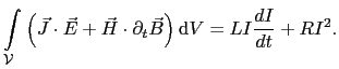
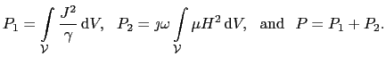
The electro-magnetic power in the domain
![]() can
be expressed in two different ways. The first one is by volume integration
over the power density distribution [103] in the
region
can
be expressed in two different ways. The first one is by volume integration
over the power density distribution [103] in the
region
![]() . The
second one is by the current flowing trough the resulting resistance and
inductance. As aforementioned, the quasi-magnetostatic case is considered
. The
second one is by the current flowing trough the resulting resistance and
inductance. As aforementioned, the quasi-magnetostatic case is considered
In the frequency domain using the constitutive relations (4.7) and (4.8) one obtains
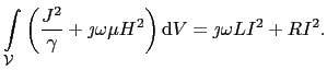
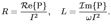
The left hand side of (6.14) can be denoted in the following way:
Consequently the resistance ![]() and the inductance
and the inductance ![]() arising in the domain
arising in the domain
![]() are calculated by
are calculated by
The domain
![]() is discretized and the linear equation system
(5.37) is assembled as described in
Section 5.2 and solved
to obtain the solution vector
is discretized and the linear equation system
(5.37) is assembled as described in
Section 5.2 and solved
to obtain the solution vector ![]() . The indexes
. The indexes ![]() of the coefficients
of the coefficients
![]() are arranged as shown in Section
5.2. The fields
are arranged as shown in Section
5.2. The fields ![]() and
and ![]() are constructed as in (5.27) and
(5.28).
are constructed as in (5.27) and
(5.28). ![]() is obtained by
(5.23). These quantities are used to determine
is obtained by
(5.23). These quantities are used to determine ![]() .
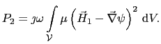
Inserting (5.13) in the expression for
.
Inserting (5.13) in the expression for ![]() from
(6.15) gives
from
(6.15) gives
or
With (5.23) ![]() is modified to read
is modified to read
Expressing ![]() from (5.27) and
from (5.27) and
![]() from (5.28) one obtains
from (5.28) one obtains
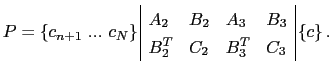
which is written in the more convenient form
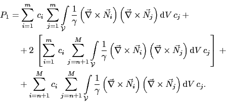
Using (6.18) and (6.21)
for ![]() and
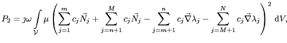
and ![]() the very suitable form for the power
the very suitable form for the power ![]() in the
simulation domain is derived
in the
simulation domain is derived
where the sub-matrices ![]() ,
, ![]() and
and ![]() with
with ![]() are calculated using the
mathematical expressions given in (5.38),
(5.39), and (5.40), respectively.
The indexes
are calculated using the
mathematical expressions given in (5.38),
(5.39), and (5.40), respectively.
The indexes ![]() of
of ![]() ,
, ![]() and
and ![]() indicate the different
ranges of the sub-matrix entries global indexes
indicate the different
ranges of the sub-matrix entries global indexes ![]() and
and ![]() . The associated
global index ranges are specified in (6.18)
and (6.21) and can be given more clearly as follows:
. The associated
global index ranges are specified in (6.18)
and (6.21) and can be given more clearly as follows:
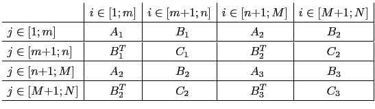 |
In (5.37)
only the
![]() part of the matrix for the unknowns is used. The remaining
part is assembled with the known Dirichlet values directly to right hand side
vector
part of the matrix for the unknowns is used. The remaining
part is assembled with the known Dirichlet values directly to right hand side
vector ![]() . For the power calculation (6.22) the whole
. For the power calculation (6.22) the whole
![]() matrix is used. Expression (6.22) can be simplified
by involving (5.37)
matrix is used. Expression (6.22) can be simplified
by involving (5.37)
![\includegraphics[width=7cm]{figures/applications/coax/coax_i_f3e7_scaled.eps}](img689.gif) |
![\includegraphics[width=7cm]{figures/applications/coax/coax_i_f3e10_scaled.eps}](img690.gif) |
![\includegraphics[width=7cm]{figures/applications/coax/coax_i_f3e11_scaled.eps}](img691.gif) |
![\includegraphics[width=7cm]{figures/applications/coax/coax_i_f3e12_scaled.eps}](img692.gif) |
![\includegraphics[width=7cm]{figures/applications/coax/coax_h_f3e7_scaled.eps}](img693.gif) |
![\includegraphics[width=7cm]{figures/applications/coax/coax_h_f3e10_scaled.eps}](img694.gif) |
![\includegraphics[width=7cm]{figures/applications/coax/coax_h_f3e11_scaled.eps}](img695.gif) |
![\includegraphics[width=7cm]{figures/applications/coax/coax_h_f3e12_scaled.eps}](img696.gif) |
![\begin{displaymath}\begin{split}P_1 & = \int_{\mathcal{V}}\frac{1}{\gamma}\left(...
...\nabla}\times\vec{N}_j\right) \right]^2 \mathrm{d}V \end{split}\end{displaymath}](img673.gif)
![\begin{displaymath}\begin{split}\frac{P_2}{\jmath\omega} & = \left.\sum_ic_i\sum...
... [m+1;n]\cup[M+1;N], j \in [m+1;n]\cup[M+1;N]}. \end{split}\end{displaymath}](img678.gif)
![$\displaystyle P = P_1 + P_2 = \left\{c\right\}^T \left[\begin{array}{llll} A_1 ...
...2 & A_3 & B_3 B_2^T & C_2 & B_3^T & C_3 \end{array}\right] \left\{c\right\},$](img679.gif)