The analytical expression for the inductance ![]() is obtained from the magnetic
energy [102]
is obtained from the magnetic
energy [102]
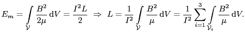
It must be distinguished between three regions: the inner conductor
![]() ,
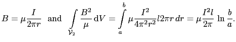
the dielectric between the conductors
,
the dielectric between the conductors
![]() , and the outer conductor
, and the outer conductor
![]() .
.
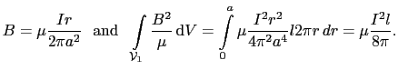
For
![]() the magnetic flux
the magnetic flux ![]() and the integral
are given by
and the integral
are given by
For
![]()
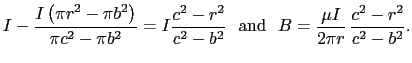
The current ![]() flows along the inner conductor. The same current returns along
the outer conductor flowing in the opposite direction. Similarly to
(6.4), for
flows along the inner conductor. The same current returns along
the outer conductor flowing in the opposite direction. Similarly to
(6.4), for
![]() where
where ![]() ,
only the current through the circle inside the integration loop must
be considered
,
only the current through the circle inside the integration loop must
be considered
Now the inductance can be obtained from the integral over the entire domain
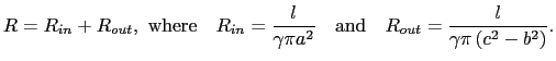
The resistance ![]() of the conductors is given by
of the conductors is given by
Equations (6.8) and (6.9) are obtained assuming a constant current density
distribution in the conductors. This is true only for low frequencies. The distinction between low and high
frequency is in terms of the skin effect. Thus, whether an operating
frequency is considered as low or high depends also on the dimensions of the
geometries, not only on the frequency itself. At high frequencies for which
skin effect is not negligible ![]() and
and ![]() are modified to read [102]
are modified to read [102]
where ![]() and
and ![]() are taken from (6.9),
are taken from (6.9), ![]() is the thickness of the outer
conductor (
is the thickness of the outer
conductor (![]() ), and the skin depth
), and the skin depth ![]() is given by the expression
is given by the expression
Notice that (6.10) and (6.11) are valid only, if ![]() is reasonably
small compared to
is reasonably
small compared to ![]() (
(![]() ).
).
![\begin{displaymath}\begin{split}\int_{\mathcal{V}_3}\frac{B^2}{\mu} \mathrm{d}V...
...eft(c^2 - b^2\right)\left(3c^2 - b^2\right)\right]. \end{split}\end{displaymath}](img656.gif)
![$\displaystyle L = \frac{\mu{}l}{2\pi{}} \left\{\frac{1}{4\pi} + \ln\frac{b}{a} ...
...{b} - \frac{1}{4}\left(c^2 - b^2\right)\left(3c^2 - b^2\right)\right] \right\}.$](img657.gif)
![$\displaystyle L = \frac{\mu{}l}{2\pi} \left\{ \frac{\delta}{2a} + \ln\frac{b}{a...
...(2\frac{d}{\delta}\right) - \cos\left(2\frac{d}{\delta}\right)\right]} \right\}$](img659.gif)
![$\displaystyle R = \frac{a}{2\delta}R_{in} + \frac{d\left[\sinh\left(2\frac{d}{\...
...t(2\frac{d}{\delta}\right) - \cos\left(2\frac{d}{\delta}\right)\right]}R_{out},$](img660.gif)
