Previous: 2.3 RESURF Up: 2.3 RESURF Next: 2.3.2 Multi-RESURF in JI
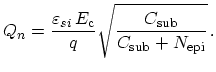
For a conventional lateral RESURF structure as shown in Figure 2.16
and at an applied reverse voltage ![]() ,
the lateral diode (
,
the lateral diode (![]() -epi) breakdown voltage
-epi) breakdown voltage
![]() and
the vertical junction (
and
the vertical junction (![]() -substrate/
-substrate/![]() -epi) depletion extension
-epi) depletion extension
![]() into
the
into
the ![]() -epi, are given by
-epi, are given by
 |
(2.6) |
 |
(2.7) |
Here,
![]() is the dielectric constant of silicon,
is the dielectric constant of silicon,
![]() is the silicon critical
electric field (
is the silicon critical
electric field (![]() 3
3 ![]()
![]() V
V![]() cm), and
cm), and ![]() is the electronic charge.
The requirement for such a structure to achieve a benefit from the RESURF principle
is that the vertical full depletion of the
is the electronic charge.
The requirement for such a structure to achieve a benefit from the RESURF principle
is that the vertical full depletion of the ![]() -epi region takes place before the lateral diode breaks down.
Since the lateral diode is the junction most susceptible to a high electric
field (i.e., represents the weakest breakdown point), this requirement causes
the electric field at that junction to reduce and leads the structure to breakdown
at a different voltage than the one predicted by (2.2). Therefore, to ensure full
vertical depletion of the
-epi region takes place before the lateral diode breaks down.
Since the lateral diode is the junction most susceptible to a high electric
field (i.e., represents the weakest breakdown point), this requirement causes
the electric field at that junction to reduce and leads the structure to breakdown
at a different voltage than the one predicted by (2.2). Therefore, to ensure full
vertical depletion of the ![]() -epi region, it is required that
-epi region, it is required that
| (2.8) |
where
![]() is the vertical depletion extension into the
is the vertical depletion extension into the
![]() -epi at
-epi at
![]() .
As a result in single-RESURF devices, the optimal
.
As a result in single-RESURF devices, the optimal ![]() -epi integrated charge
-epi integrated charge
![]()
![]()
![]()
![]()
![]() is given by
is given by
 |
(2.9) |
When processing and forming doped regions in IC technologies, and in order to
have reasonable control over the thickness and doping concentrations of
these regions, it is essential that the doping concentration of the ![]() -epi
region is higher than that of the
-epi
region is higher than that of the ![]() -substrate. In other words,
-substrate. In other words,
![]() .
Consequently, an upper theoretical bound for
.
Consequently, an upper theoretical bound for ![]() can be obtained by setting
can be obtained by setting
![]() in (2.9) which is given by
in (2.9) which is given by
 |
(2.10) |
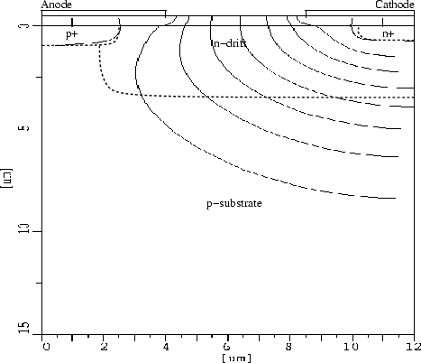
Figure 2.18 and Figure 2.19 show the
optimum potential distribution and electric field strength of
150V lateral ![]() -diode with drift length
-diode with drift length
![]()
![]() 7
7![]() m, respectively.
Generally, electric fields are focused at the anode and cathode edge.
m, respectively.
Generally, electric fields are focused at the anode and cathode edge.
 |
Field plates are introduced to reduce the electric fields
at these region. Without a field plate at the anode region the required ![]() -drift doping will
be lowered, which significantly increases the on-resistance. In addition the BV
will decrease due to the field crowding at the anode and cathode edges.
From Figure 2.18, almost uniformly distributed potential lines of the
lateral diode can be seen at a cathode voltage of 150V (optimum doping of
the
-drift doping will
be lowered, which significantly increases the on-resistance. In addition the BV
will decrease due to the field crowding at the anode and cathode edges.
From Figure 2.18, almost uniformly distributed potential lines of the
lateral diode can be seen at a cathode voltage of 150V (optimum doping of
the ![]() -drift is
-drift is
![]()
![]() ). The
theoretical maximum BV is determined by the breakdown of the vertical
diode structure (by the depletion layer width at the
). The
theoretical maximum BV is determined by the breakdown of the vertical
diode structure (by the depletion layer width at the ![]() -sub
and
-sub
and ![]() -drift junction).
-drift junction).
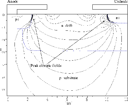
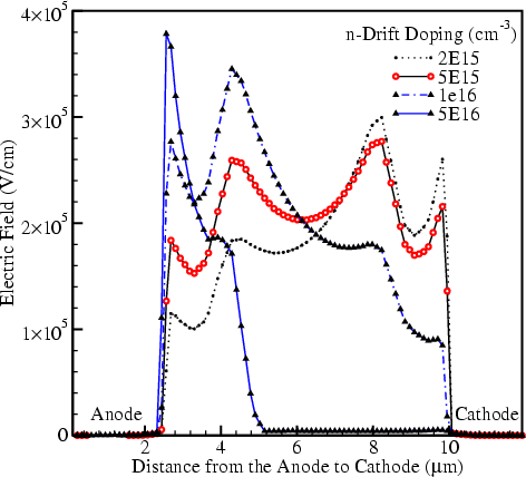
Figure 2.19 shows the ![]() -drift doping dependence of the electric field
strength near the surface of the device. At the cathode edge a high
electric field can be seen with a low
-drift doping dependence of the electric field
strength near the surface of the device. At the cathode edge a high
electric field can be seen with a low ![]() -drift doping
of 2
-drift doping
of 2 ![]()
![]()
![]() , and if the
, and if the ![]() -drift doping is increased
to
-drift doping is increased
to ![]()
![]() , a high
electric field is moved toward the anode edge. The optimum electric
field distribution is obtained with an
, a high
electric field is moved toward the anode edge. The optimum electric
field distribution is obtained with an ![]() -drift doping of 5
-drift doping of 5 ![]()
![]()
![]() .
At this optimum doping the peak electric field can be seen both at the anode and
cathode edge, and the distribution between them forms a parabolic shape.
It shows that the optimum RESURF condition can be obtained
with an
.
At this optimum doping the peak electric field can be seen both at the anode and
cathode edge, and the distribution between them forms a parabolic shape.
It shows that the optimum RESURF condition can be obtained
with an ![]() -drift doping higher than that of the
-drift doping higher than that of the ![]() -substrate.
-substrate.
With the higher ![]() -drift dose the peak electric field occurs
only at the
-drift dose the peak electric field occurs
only at the ![]() -drift junction (dotted line in Figure 2.19)
of the anode side, and the BV decreases. The vertical diode depletes
rapidly, and the electric field at the anode side exceeds critical
value of silicon before the lateral depletion is achieved.
Therefore, a premature breakdown occur at the surface of the
-drift junction (dotted line in Figure 2.19)
of the anode side, and the BV decreases. The vertical diode depletes
rapidly, and the electric field at the anode side exceeds critical
value of silicon before the lateral depletion is achieved.
Therefore, a premature breakdown occur at the surface of the ![]() -junction.
-junction.
With the lower ![]() -drift doping the peak electric field moves
towards
-drift doping the peak electric field moves
towards ![]() -cathode. It causes a BV lower (dashed line in Figure 2.19).
If the
-cathode. It causes a BV lower (dashed line in Figure 2.19).
If the ![]() -drift doping is lower compared to that of the
-drift doping is lower compared to that of the ![]() -substrate,
depletion mainly occurs in the
-substrate,
depletion mainly occurs in the ![]() -drift region and the BV decreases.
The optimal case is obtained when the depletion region extends
equally in the
-drift region and the BV decreases.
The optimal case is obtained when the depletion region extends
equally in the ![]() -drift and
-drift and ![]() -substrate regions.
If the lateral distance is sufficient, breakdown occurs vertically
in the semiconductor bulk under the
-substrate regions.
If the lateral distance is sufficient, breakdown occurs vertically
in the semiconductor bulk under the ![]() -region.
Figure 2.20 shows the electric field distribution of the optimized lateral diode,
where the peak electric field can be seen under the cathode edge.
-region.
Figure 2.20 shows the electric field distribution of the optimized lateral diode,
where the peak electric field can be seen under the cathode edge.
Jong-Mun Park 2004-10-28