Previous: 2.2.4 Double Gate Lateral Inversion Layer Emitter Transistor Up: 2. Background Survey of Power Devices and Related Next: 2.3.1 Conventional RESURF in JI
High-voltage devices usually require thick and low doped epitaxial layer,
which makes them difficult to integrate with
low-voltage circuitry. Because of the high-resistivity epitaxial layer, the
on-state resistances of such devices is large.
In 1979 Appels and Vaes suggested the reduced surface field (RESURF) concept [106].
The RESURF concept [107] gives the best trade-off between the breakdown voltage and the
on-resistance of lateral devices.
It has been shown that a lateral diode with a thin ![]() -type epitaxial layer on a
lowly doped
-type epitaxial layer on a
lowly doped ![]() -substrate can give a higher breakdown voltage than a conventional lateral diode.
-substrate can give a higher breakdown voltage than a conventional lateral diode.
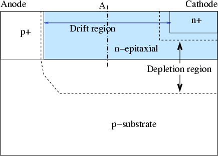
As shown in Figure 2.16 for a certain range of the
![]() -epitaxial (drift region) thickness and doping, the depletion
region covers almost all the area of the thin epitaxial layer. It allows
the depletion region to extend further than for the corresponding
one-dimensional lateral diode without
-epitaxial (drift region) thickness and doping, the depletion
region covers almost all the area of the thin epitaxial layer. It allows
the depletion region to extend further than for the corresponding
one-dimensional lateral diode without ![]() -substrate. As a result the surface field
is decreased, and higher voltages can be applied to the devices.
This is the well known RESURF effect.
For an optimum doping and thickness of the
-substrate. As a result the surface field
is decreased, and higher voltages can be applied to the devices.
This is the well known RESURF effect.
For an optimum doping and thickness of the ![]() -layer, a uniformly distributed
voltage across the silicon surface in the drift region can be seen and
a bulk breakdown voltage can be achieved. The breakdown voltage of lateral
RESURF devices is limited by the substrate doping.
-layer, a uniformly distributed
voltage across the silicon surface in the drift region can be seen and
a bulk breakdown voltage can be achieved. The breakdown voltage of lateral
RESURF devices is limited by the substrate doping.
The charge of the ![]() -layer determines the resistance of the drift region
which is the most critical parameter of high-voltage devices.
Together with the length of the drift region it will determine the on-resistance
and current handling capability of the device.
-layer determines the resistance of the drift region
which is the most critical parameter of high-voltage devices.
Together with the length of the drift region it will determine the on-resistance
and current handling capability of the device.
The RESURF technology has been one of the most frequently applied methods for the design of high-voltage lateral devices with low on-resistance [107,108,109,110]. It has been successfully used for lateral high-voltage devices such as diodes and LDMOS transistors for 20 - 1200V. This technology provides an efficient way to integrate high-voltage devices with low voltage circuitry.
The traditional RESURF structure is constructed by a
lateral ![]() -diode (
-diode (![]() -epitaxial, see Figure 2.16) that defines
the on-resistance characteristic of
the device and a vertical
-epitaxial, see Figure 2.16) that defines
the on-resistance characteristic of
the device and a vertical ![]() -diode which supports a
space charge depletion region enabling high BV.
-diode which supports a
space charge depletion region enabling high BV.
The lateral BV of this structure depends on the ![]() -epi net charge of the drift region,
which is given when the
-epi net charge of the drift region,
which is given when the ![]() -epi net doping is integrated from
the surface to the vertical
-epi net doping is integrated from
the surface to the vertical ![]() -junction (
-junction (![]() -substrate/
-substrate/![]() -epi) along the cut
line A in Figure 2.16.
Assuming that the
-epi) along the cut
line A in Figure 2.16.
Assuming that the ![]() -epi layer in Figure 2.16 is fully depleted with
optimum drift dose, the maximum BV is
determined by the BV of the vertical
-epi layer in Figure 2.16 is fully depleted with
optimum drift dose, the maximum BV is
determined by the BV of the vertical ![]() -diode (
-diode (![]() -substrate/
-substrate/![]() -epitaxial).
The drift region resistance is inversely proportional to the net charge in this region.
Due to the vertical junction of the RESURF structure, a second electric field
peak forms at the
-epitaxial).
The drift region resistance is inversely proportional to the net charge in this region.
Due to the vertical junction of the RESURF structure, a second electric field
peak forms at the ![]() -cathode end of the device.
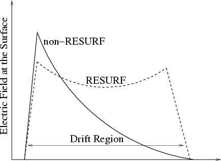
As shown in Figure 2.17 the electric field at the surface of the
RESURF device (after full depletion) assumes a parabolic
rather than a linear distribution
which can be seen in conventional high-voltage devices. It helps to reduce the electric field
at the surface of the device during off-state.
-cathode end of the device.
As shown in Figure 2.17 the electric field at the surface of the
RESURF device (after full depletion) assumes a parabolic
rather than a linear distribution
which can be seen in conventional high-voltage devices. It helps to reduce the electric field
at the surface of the device during off-state.
The basic properties of RESURF structures are
determined by the ![]() -substrate
doping concentration (
-substrate
doping concentration (
![]() ), the
), the ![]() -epi layer doping
concentration (
-epi layer doping
concentration (
![]() ), and the
), and the ![]() -epi layer thickness (
-epi layer thickness (
![]() ).
In the structure shown in Figure 2.16, an approximate net charge
).
In the structure shown in Figure 2.16, an approximate net charge ![]() of
the
of
the ![]() -epi layer (assuming uniform doping) is given by
-epi layer (assuming uniform doping) is given by
| (2.5) |
The BV performance depends significantly on the net charge ![]() of the
of the
![]() -epi layer.
The optimum
-epi layer.
The optimum ![]() is found by assuming that the vertical depletion
must reach the surface before the lateral junction breaks down.
The vertical space charge width in the
is found by assuming that the vertical depletion
must reach the surface before the lateral junction breaks down.
The vertical space charge width in the ![]() -epi region extends and interacts
with the lateral junction space charge region allowing the lateral depletion width to effectively
span a larger distance compared to the case without the presence of the
-epi region extends and interacts
with the lateral junction space charge region allowing the lateral depletion width to effectively
span a larger distance compared to the case without the presence of the ![]() -substrate.
As a result, the lateral electric field at the lateral
-substrate.
As a result, the lateral electric field at the lateral ![]() -epi junction is
significantly reduced relative to the one-dimensional diode case,
therefore enabling higher voltages to be applied.
Consequently, to achieve a high BV in RESURF structures,
it is required that the
-epi junction is
significantly reduced relative to the one-dimensional diode case,
therefore enabling higher voltages to be applied.
Consequently, to achieve a high BV in RESURF structures,
it is required that the ![]() -epi region is fully depleted before the lateral electric
field reaches a critical value.
-epi region is fully depleted before the lateral electric
field reaches a critical value.