Previous: 3.2.1.2 Closed Form of the BV and On-Resistance Up: 3.2 Device Characteristics for Power Semiconductor Devices Next: 3.2.3 Parasitic and Transistors in Smart Power ICs
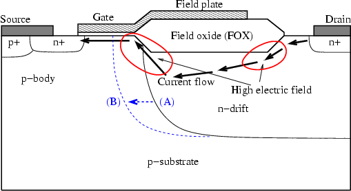
When carriers in silicon gain energy above a certain threshold, they can generate electron-hole pairs through impact-ionization. Figure 3.8 shows the location of high electric field inside an LDMOSFET. As shown in the figure high impact ionization due to high electric field can be seen at the gate edge of the drain side and at the drain edge of the device.
Normally an electric field at the gate edge of drain side
(practically the bird's beak area of the LDMOSFET)
are high at low gate to source voltage
![]() .
The carriers in this region generated by impact ionization can
themselves gain enough energy (called hot carriers) to be
injected into the gate oxide. For high-voltage LDMOSFETs a high electric field
under the bird's beak between the field oxide (FOX) and the gate oxide
is the major source of the device degradation by the hot carriers.
If the gate voltage is increased (or current is increased), the area of high electric field
is moved towards drain.
.
The carriers in this region generated by impact ionization can
themselves gain enough energy (called hot carriers) to be
injected into the gate oxide. For high-voltage LDMOSFETs a high electric field
under the bird's beak between the field oxide (FOX) and the gate oxide
is the major source of the device degradation by the hot carriers.
If the gate voltage is increased (or current is increased), the area of high electric field
is moved towards drain.
Carriers near the
![]() and
and
![]() interface have to overcome
an energy barrier in order to enter the oxide.
interface have to overcome
an energy barrier in order to enter the oxide.
![]() has an electron affinity of 0.9eV and a bandgap of approximately 9.0eV.
Similarly,
has an electron affinity of 0.9eV and a bandgap of approximately 9.0eV.
Similarly,
![]() has an electron affinity of 4.05eV and a bandgap of 1.12eV.
The band alignment at the
has an electron affinity of 4.05eV and a bandgap of 1.12eV.
The band alignment at the
![]() and
and
![]() interface thus results
in an energy barrier of about 3.1eV for electrons and 4.8eV for holes.
As a result of the large difference between the energy barriers for electrons and holes,
under similar conditions, electrons will be injected into
interface thus results
in an energy barrier of about 3.1eV for electrons and 4.8eV for holes.
As a result of the large difference between the energy barriers for electrons and holes,
under similar conditions, electrons will be injected into
![]() in much
larger quantities than holes.
in much
larger quantities than holes.
These injected hot carriers interact with the oxide and generate defects in the
oxide and at the
![]() and
and
![]() interface. The traps created by
this process collect charge over time and directly affect the device operation.
interface. The traps created by
this process collect charge over time and directly affect the device operation.
Extensive research has been undertaken to minimize the degradation effects by
hot carrier injection [119,120,121,122,123].
Several fabrication steps were
suggested to minimize hot carrier effects in LDMOSFETs. One way is
to reduce the number of trapping centers at the gate oxide and silicon interface.
To achieve this, a low temperature gate oxidation (long
annealing at the end of gate oxidation) can be used and the gate oxidation process can be
chemically enhanced by incorporating
![]() ,
,
![]() and
and
![]() . These
elements strengthen the
. These
elements strengthen the
![]() -
-
![]() bond at the gate
oxide and silicon interface.
bond at the gate
oxide and silicon interface.
From the point of device design, hot carrier generation can be minimized by using various RESURF techniques in order to reduce the electric field at the interface of the device. In addition moving the current path away from the high electric field and the impact ionization region deep into the silicon instead of the surface can help to reduce hot carrier degradation of the device.
The LDD (lightly doped drain), stepped gate extention structure, and proper design of the field plate can be used to optimize the surface electric field of a RESURF device, hence reducing device degradation by hot carriers.
By simply changing the ![]() -body and
-body and ![]() -drift junction from (A) to (B) (see Figure 3.8),
the high impact ionization zone is moved to the bulk instead of the surface under the bird's beak.
It will greatly reduce the hot carrier generation at the bird's beak region of the device.
-drift junction from (A) to (B) (see Figure 3.8),
the high impact ionization zone is moved to the bulk instead of the surface under the bird's beak.
It will greatly reduce the hot carrier generation at the bird's beak region of the device.
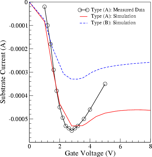
Some of the hot carriers generated at the bird's beak area are injected into the gate oxide and the others constitute the substrate current. The majority of hot carriers injected into the gate oxide is collected by the gate electrode and constitute the gate current. Both of the gate current and substrate current are a good monitor to predict device degradation. While gate current is a direct measurement of the injected carriers into the gate oxide, it is very sensitive to the trapping mechanism (during TCAD simulation) and is very low. On the other hand, substrate current is much larger than the gate current and it makes easier to measure. Although high-voltage LDMOSFETs have a large depletion area in the drift region (large part of the generation current by impact ionization in this region constitute a substrate current), substrate current is an indirect way of measuring the hot carrier injection.
Figure 3.9 shows the substrate current versus
![]() of type (A) and (B)
in Figure 3.8 at the
of type (A) and (B)
in Figure 3.8 at the
![]() = 55V. One can see the large amount
of substrate current for the device type (A) (circle: measured values,
red solid line: simulated values).
With type (B) substrate current (dashed line: simulated values) was greatly
reduced approximately from - 0.00055A to - 0.00033A.
We have investigated a variety of RESURF structures to reduce the surface electric field.
It will be shown in Chapter 4 that the surface electric fields of our suggested devices
are further reduced by SJ and lateral trench gate concepts together with RESURF principle.
= 55V. One can see the large amount
of substrate current for the device type (A) (circle: measured values,
red solid line: simulated values).
With type (B) substrate current (dashed line: simulated values) was greatly
reduced approximately from - 0.00055A to - 0.00033A.
We have investigated a variety of RESURF structures to reduce the surface electric field.
It will be shown in Chapter 4 that the surface electric fields of our suggested devices
are further reduced by SJ and lateral trench gate concepts together with RESURF principle.
Jong-Mun Park 2004-10-28