Previous: 3.2.2 Hot Carrier Effect in LDMOSFETs Up: 3.2 Device Characteristics for Power Semiconductor Devices Next: 3.3 Super-Junction Concepts
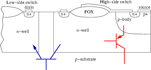
Figure 3.10 shows the schematic structure of
parasitic ![]() and
and ![]() transistors in LDMOSFETs. When an inductive
load is switched by LDMOSFETs, the potential of the drain (
transistors in LDMOSFETs. When an inductive
load is switched by LDMOSFETs, the potential of the drain (![]() at
the low-side switch in the figure) can dive below the ground potential of
at
the low-side switch in the figure) can dive below the ground potential of ![]() -substrate.
Under this condition a considerable amount of electrons is injected into the substrate.
These electrons either recombine with holes in the substrate or they are collected by another
-substrate.
Under this condition a considerable amount of electrons is injected into the substrate.
These electrons either recombine with holes in the substrate or they are collected by another
![]() -well of LDMOSFETs or logic CMOS. The substrate doping concentration and minority
carrier lifetime in this region play a major role in the behavior of this parasitic
-well of LDMOSFETs or logic CMOS. The substrate doping concentration and minority
carrier lifetime in this region play a major role in the behavior of this parasitic
![]() -structure. With a high doping concentration and shorter minority carrier lifetime of the
substrate, the parasitic
-structure. With a high doping concentration and shorter minority carrier lifetime of the
substrate, the parasitic ![]() -structure is suppressed significantly.
-structure is suppressed significantly.
At the same time the potential of a source of the high-side switch
(![]() in the
in the ![]() -body) can be over supply voltage, and the
-body) can be over supply voltage, and the ![]() -body
contact at the source side injects holes into the
-body
contact at the source side injects holes into the ![]() -well. Most of these
holes recombine in the
-well. Most of these
holes recombine in the ![]() -well with electrons, but some reach the substrate.
If the
-well with electrons, but some reach the substrate.
If the ![]() -well doping is increased, this parasitic
-well doping is increased, this parasitic ![]() -transistor
gain can be suppressed.
-transistor
gain can be suppressed.
The electrons and holes injected into the substrate can cause the latch-up of LDMOSFETs
themselves, or they are collected by an ![]() -well of the CMOS structure and can induce
latch-up [124]. With the SOI or deep trench isolation the substrate current of
a smart power IC can be effectively suppressed.
-well of the CMOS structure and can induce
latch-up [124]. With the SOI or deep trench isolation the substrate current of
a smart power IC can be effectively suppressed.
Jong-Mun Park 2004-10-28