Previous: 4.1.3 Simulation Results Up: 4.1.3 Simulation Results Next: 4.1.3.2 Temperature Dependence of the Device Characteristics and
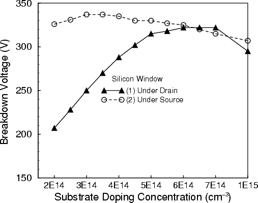
The simulated BVs of P-SOI LDMOSFETs as a function of the
substrate doping concentration
![]() are shown in Figure 4.4.
The BV increases with increasing
are shown in Figure 4.4.
The BV increases with increasing
![]() for the P-SOI with a
silicon window under the drain, because the RESURF condition of the SOI
structure is affected by
for the P-SOI with a
silicon window under the drain, because the RESURF condition of the SOI
structure is affected by
![]() . Below a
. Below a
![]() of 4
of 4 ![]()
![]()
![]() in this structure, the BV is lower than that of conventional SOI-LDMOSFETs.
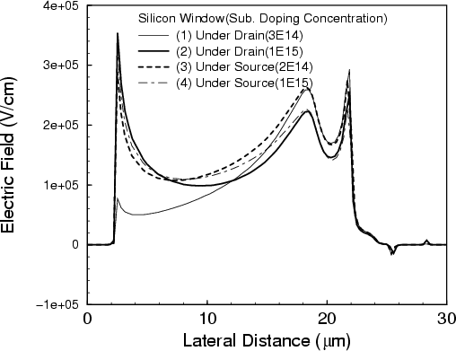
The solid lines in Figure 4.5 show the electric field near the surface
with substrate doping levels of 3
in this structure, the BV is lower than that of conventional SOI-LDMOSFETs.
The solid lines in Figure 4.5 show the electric field near the surface
with substrate doping levels of 3 ![]()
![]()
![]() and 1
and 1 ![]()
![]()
![]() ,
respectively.
,
respectively.
At the gate edge (near the lateral distance of 21![]() m
in Figure 4.5),
a high electric field can be seen with a low substrate doping
concentration
m
in Figure 4.5),
a high electric field can be seen with a low substrate doping
concentration
![]() of 3
of 3 ![]()
![]()
![]() and only a low
electric field is found at the drain edge (near the lateral distance
of 2
and only a low
electric field is found at the drain edge (near the lateral distance
of 2![]() m in Figure 4.5).
It means that the RESURF condition strongly depends on
m in Figure 4.5).
It means that the RESURF condition strongly depends on
![]() in this structure.
Further increasing
in this structure.
Further increasing
![]() over 7
over 7 ![]()
![]()
![]() reduces the depletion
layer width in the substrate region, which decreases the BV (solid line
in Figure 4.4). The buried oxide layer does not affect the BV.
reduces the depletion
layer width in the substrate region, which decreases the BV (solid line
in Figure 4.4). The buried oxide layer does not affect the BV.
In the P-SOI with a silicon window under the source, the RESURF condition does
not depend on the substrate doping concentration (from 2 ![]()
![]()
![]() to 1
to 1 ![]()
![]()
![]() ) as shown by the dashed lines in Figure 4.4
and Figure 4.5.
However, the BV decreases slowly with increasing
) as shown by the dashed lines in Figure 4.4
and Figure 4.5.
However, the BV decreases slowly with increasing
![]() because of the
reduced depletion layer width in the substrate region.
because of the
reduced depletion layer width in the substrate region.
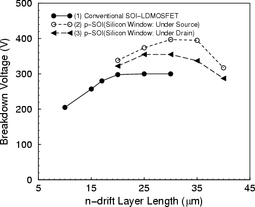
BV versus ![]() -drift layer length
-drift layer length
![]() is shown in Figure 4.6.
The maximum BV of the conventional SOI LDMOSFET is 300V at
is shown in Figure 4.6.
The maximum BV of the conventional SOI LDMOSFET is 300V at
![]()
![]() 20
20![]() m which
does not change by increasing the
m which
does not change by increasing the ![]() -drift layer length from 20
-drift layer length from 20![]() m to 30
m to 30![]() m.
The maximum voltage is limited by the RESURF condition of the SOI in this structure.
In the P-SOI with a silicon window under the drain, the BV is determined by both
the RESURF condition and the depletion layer width of the substrate. The maximum
BV of this structure is 355V at
m.
The maximum voltage is limited by the RESURF condition of the SOI in this structure.
In the P-SOI with a silicon window under the drain, the BV is determined by both
the RESURF condition and the depletion layer width of the substrate. The maximum
BV of this structure is 355V at
![]()
![]() 6
6 ![]()
![]()
![]() and
and
![]()
![]() 25
25![]() m.
The improvement in the voltage handling capability is about 18%. Further
increasing
m.
The improvement in the voltage handling capability is about 18%. Further
increasing
![]() over 30
over 30![]() m decreases the BV by the RESURF condition.
m decreases the BV by the RESURF condition.
In the P-SOI with a silicon window under the source both, the buried oxide and
the depletion region of the substrate, help to increase the BV. A maximum BV
of 397V is obtained
at
![]()
![]() 3
3 ![]()
![]()
![]() and
and
![]()
![]() 30
30![]() m.
The improvement in the voltage handling capability is about 32% compared
to the conventional 300V SOI-LDMOSFET. Because part of the voltage drops in
the buried oxide and in the depletion layer in the substrate region, a higher BV
is obtained in this structure compared to that of the P-SOI with the
silicon window under the drain.
m.
The improvement in the voltage handling capability is about 32% compared
to the conventional 300V SOI-LDMOSFET. Because part of the voltage drops in
the buried oxide and in the depletion layer in the substrate region, a higher BV
is obtained in this structure compared to that of the P-SOI with the
silicon window under the drain.
Jong-Mun Park 2004-10-28