Process operations include ion implantation for the introduction of dopant materials into the semiconductor substrate, thermal treatments to induce dopant diffusion and oxidation processes, etch and deposition processes to structure the semiconductor surface, spin-on processes to create resist coatings and protective films, optical and other varieties of lithography processes to transfer patterns from masks onto the semiconductor surface to determine the affected regions for subsequent etch and ion implantation processes, chemical-mechanical polishing (CMP) to create an even wafer surface, and others. See [Rug84] [WT86] [Sze88] for a more detailed discussion.
These processes can roughly be subdivided into four main groups that are used (1) to build material layers atop the wafer surface, (2) to transfer geometrical patterns onto the wafers surface, (3) to etch and remove material from the exposed part of the wafer, and (4) to incorporate doping in the wafer bulk. Table 5.1 gives a short list of common fabrication processes.
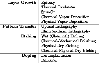
Table 5.1: Examples of VLSI fabrication processes.
In addition to these primary types of process operations, other treatments are applied to the wafer to remove dust and oxides from the surface, to increase surface adhesion for subsequent coatings, to harden resist coatings by baking, etc. They do not serve a particular purpose in altering the wafer's surface geometry or in modifying the distribution of dopants in its interior, but are necessary to ensure the smooth and reliable operation of the primary treatments. As a consequence, these steps are usually not explicitly referred to when a process technology is discussed. Nevertheless, their importance for manufacturing must not be underestimated, and they play a crucial role in achieving a sufficiently high yield.