In current integrated circuits contacts have to fulfill a long list of
requirements: The contact resistivity has to be low, the metallurgical
isolation which prohibits the diffusion of the contact metal into the silicon
has to be guaranteed, the adhesion has to be sufficient, and leakage free film
formation as well as void free filling has to be assured. It is clear, that the
complete list cannot be fulfilled by a single material but only by a compound
of different layers which perform different tasks. For metal stacks used for
tungsten plug fills, ![]() has been recognized as excellent barrier material
and is used as nucleation/glue layer at the contact/via level as well as a
diffusion barrier and anti-reflection coating in the interconnect
stack [14].
has been recognized as excellent barrier material
and is used as nucleation/glue layer at the contact/via level as well as a
diffusion barrier and anti-reflection coating in the interconnect
stack [14].
Several physical vapor deposition techniques, such as magnetron sputter
deposition [58], collimated sputtering [61], and reactive
sputtering [11] as well as chemical vapor deposition
techniques [15] exist for the deposition of ![]() and are selected
depending on the purpose of the layer. Our general approach can model different
physical deposition techniques, since it approximates the particle
distributions arriving at the wafer surface, regardless of the processes
occurring in the reactor chamber, which are responsible for the incidence
characteristics.
and are selected
depending on the purpose of the layer. Our general approach can model different
physical deposition techniques, since it approximates the particle
distributions arriving at the wafer surface, regardless of the processes
occurring in the reactor chamber, which are responsible for the incidence
characteristics.
As explained in Section 6.1.4 a detailed model taking into account direct and reflected contributions of different types of particles results in a huge amount of distribution and interaction parameters which are usually hard to assess. Therefore an overall fitting approach was selected in order to model magnetron sputter deposition.
The ![]() particles ejected from the target react with the argon/nitrogen plasma
and arrive at the wafer surface as
particles ejected from the target react with the argon/nitrogen plasma
and arrive at the wafer surface as ![]() particles. According to the reactor
configuration from Fig. 6.4 with the circular racetrack in the sputter
target (6.4) was used to approximate the incoming distribution of the
particles. According to the reactor
configuration from Fig. 6.4 with the circular racetrack in the sputter
target (6.4) was used to approximate the incoming distribution of the
![]() particles. The equation was extended to
particles. The equation was extended to
Thus, there are only two free parameters left for the distribution function. The
first one is the angle of maximum particle incidence, which is converted to the
parameters ![]() and
and ![]() in (6.15). As a first approximation this angle
is given by the direction of the maximum depth in the target erosion profile
seen from the center of the wafer. Due to the uncertainty in the determination
of the maximum of the shallow erosion profile and the additional collisions of
the particles on their way from the target to the wafer, the angle does not
necessarily correspond to the geometric angle and was left as a variable for
the following optimization. The second parameter is the fraction of low energy
particles, given by the parameter
in (6.15). As a first approximation this angle
is given by the direction of the maximum depth in the target erosion profile
seen from the center of the wafer. Due to the uncertainty in the determination
of the maximum of the shallow erosion profile and the additional collisions of
the particles on their way from the target to the wafer, the angle does not
necessarily correspond to the geometric angle and was left as a variable for
the following optimization. The second parameter is the fraction of low energy
particles, given by the parameter ![]() .
. ![]() in (6.15) is kept constant
at a value of 5 accounting for a fast increase of the low energy fraction
from 0 for normal incidence to its nominal value
in (6.15) is kept constant
at a value of 5 accounting for a fast increase of the low energy fraction
from 0 for normal incidence to its nominal value ![]() for an incidence angle of
90
for an incidence angle of
90![]() .
.
![\begin{figure}
% latex2html id marker 4537
\psfrag{angle}[][]{$\vartheta$ [$^\c...
...\includegraphics[width=0.6\textwidth]{eps-pvd/exp.eps}}
\end{center}\end{figure}](img315.gif) |
Fig. 6.15 shows three set of curves for distribution functions which represent different process pressures (cf. Section 6.1.2). The solid lines represent the overall distribution function according to (6.15), which is composed by the contribution of (6.4) (dashed lines) plus the additive term for the low energy particle fraction (dotted lines).
With this one-species model the barrier layer formation for a series of vias
with different diameters ranging from 0.3![]() to 1.0
to 1.0![]() was simulated at a
center wafer position and 90mm off the wafer center. The deposition was
performed at a deposition rate of 33.8nm/min for 320s. The depth of the
vias is 1.3
was simulated at a
center wafer position and 90mm off the wafer center. The deposition was
performed at a deposition rate of 33.8nm/min for 320s. The depth of the
vias is 1.3![]() for all diameters. The final goal of the simulations was to
calibrate the model with experimentally obtained profiles for the circular vias
and to subsequently use the calibrated model to predict possible leakages in
the barrier layer formation when applying the same process technology to a
damascene structure. The pressure for the experiments was 2.3mTorr, which
matches exactly the pressure region for the MC particle transport simulations
from [46], building the base for the assumed distribution function.
for all diameters. The final goal of the simulations was to
calibrate the model with experimentally obtained profiles for the circular vias
and to subsequently use the calibrated model to predict possible leakages in
the barrier layer formation when applying the same process technology to a
damascene structure. The pressure for the experiments was 2.3mTorr, which
matches exactly the pressure region for the MC particle transport simulations
from [46], building the base for the assumed distribution function.
For the calibration with the optimization tool
SIESTA [54][76], the simulation results of the 1.0![]() structure were compared with experimentally obtained film thicknesses extracted
from SEM cross-sections. This was done for the center wafer position as well as
for the off-center position. The calibration was restricted to the 1.0
structure were compared with experimentally obtained film thicknesses extracted
from SEM cross-sections. This was done for the center wafer position as well as
for the off-center position. The calibration was restricted to the 1.0![]() structure because it shows the largest film thickness and hence introduces the
lowest error in the measurement of the profiles. Furthermore the restriction to
one diameter allowed the validation of the calibration with the other four
diameters (0.3, 0.4, 0.5, and 0.7
structure because it shows the largest film thickness and hence introduces the
lowest error in the measurement of the profiles. Furthermore the restriction to
one diameter allowed the validation of the calibration with the other four
diameters (0.3, 0.4, 0.5, and 0.7![]() ).
).
By adjusting the two free parameters of the distribution function, namely, the
angle of maximum particle incidence and the fraction of laterally incident
particles, the optimization minimizes the difference between calculated film
thicknesses and thicknesses extracted from the SEM profiles. The results from
the optimization are 9.2![]() for the angular position of the maximum in the
distribution function and 0.12 for the fraction of lateral particles.
for the angular position of the maximum in the
distribution function and 0.12 for the fraction of lateral particles.
![\begin{figure}\psfrag{0}{}\psfrag{1.8}{}\psfrag{0.7}{}\psfrag{-0.7}{}\psfrag{[\2...
...graphics[width=0.22\textwidth]{eps-pvd/pH_07_bw.eps}}
}
\end{center}\end{figure}](img317.gif) |
Fig. 6.16 compares simulated and experimental cross-sections for the
structures with 0.4 and 0.7![]() diameter. The simulations have been carried
out with the parameters obtained from the calibration with the 1.0
diameter. The simulations have been carried
out with the parameters obtained from the calibration with the 1.0![]() structure. It is clear, that the calibrated 1.0
structure. It is clear, that the calibrated 1.0![]() structure exactly matches
the SEM cross-sections, therefore the comparison is omitted. The figures for
the simulation results are cross-sections through the three-dimensional
simulation domains. Three-dimensional simulations were necessary for the
correct visibility conditions for the three-dimensional distribution
functions. The cross-sections were extracted with an auxiliary function of the
solid modeling tool introduced in Chapter 3.
structure exactly matches
the SEM cross-sections, therefore the comparison is omitted. The figures for
the simulation results are cross-sections through the three-dimensional
simulation domains. Three-dimensional simulations were necessary for the
correct visibility conditions for the three-dimensional distribution
functions. The cross-sections were extracted with an auxiliary function of the
solid modeling tool introduced in Chapter 3.
The figures demonstrate, that the simulated profiles are in excellent agreement with the SEM cross-sections. The simulation results represent the downward decrease in the sidewall thickness as well as the curvature at the bottom of the via. The figures in the upper row show the center wafer position with radially symmetric profiles. The lower row demonstrates the results for the position 90mm off the wafer center. The right side of the structures is exposed towards the slanted particle flux, whereas for the sidewall on the left hand side a major part of the flux is screened, which leads to a strongly asymmetric profile. Regardless of the polar position of the radially symmetric structures, the side which is facing towards the center of the wafer exhibits the larger thickness, the side looking away from the wafer center resides in the shadow of the flux, which leads to a lower film thickness.
For the constant depth of 1.3![]() for the vias, the aspect ratio defined as
the ratio between depth and width of the structure increases for decreasing
diameters of the vias and the opening angle towards the particle source
decreases. In consequence, the film thickness at the bottom is decreasing when
the diameter becomes smaller. Still, bottom coverage is assured for all
diameters and the deposited film is thick enough to insure a sufficient barrier
function of the layer.
for the vias, the aspect ratio defined as
the ratio between depth and width of the structure increases for decreasing
diameters of the vias and the opening angle towards the particle source
decreases. In consequence, the film thickness at the bottom is decreasing when
the diameter becomes smaller. Still, bottom coverage is assured for all
diameters and the deposited film is thick enough to insure a sufficient barrier
function of the layer.
With the same parameters, a damascene structure consisting of a 0.3![]() diameter, 0.7
diameter, 0.7![]() deep hole in a 0.3
deep hole in a 0.3![]() wide, 0.5
wide, 0.5![]() deep rectangular
trench was simulated. For this structure which combines a radially symmetric
feature with a trench considered as infinitely long, a three-dimensional
simulation is absolutely necessary. Furthermore the orientation of the trench
with respect to the main particle incidence and thus the polar
position
deep rectangular
trench was simulated. For this structure which combines a radially symmetric
feature with a trench considered as infinitely long, a three-dimensional
simulation is absolutely necessary. Furthermore the orientation of the trench
with respect to the main particle incidence and thus the polar
position ![]() of the structure on the wafer is of significant influence.
of the structure on the wafer is of significant influence.
![\begin{figure}\psfrag{Pos1}[rb][rb][1.0]{{\Large\bf Pos. 1}}
\psfrag{Pos2}[lt][...
...phics[width=0.6\textwidth,clip]{eps-pvd/positions.eps}}
\end{center}\end{figure}](img318.gif) |
For these reasons, the damascene structure has been simulated for different positions on the wafer. The most pronounced differences can be found between the two positions shown in Fig. 6.17. Pos.1 is located at a peripheral position right from the wafer center. Thus, the main particle incidence for this position (indicated in the figure by the thick, black arrow) is oriented perpendicularly to the trench. This is opposed to Pos.2 which is located behind the wafer center. In this case the orientation of the trench is the same as for Pos.1, but since the particle incidence predominantly originating from the center of the wafer changes its direction, the flux is now oriented parallelly to the trench.
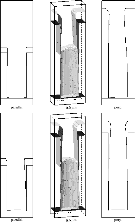 |
Fig. 6.18 shows the simulation results for the damascene structure at the two different off-center positions. For both positions the resulting three-dimensional topography and cross-sections parallel (left) and perpendicular (right) to the trench are shown. For the direction and the position of the cross-sections refer to Fig. 6.17. The three figures in the upper row represent Pos.1, the other three figures stand for a damascene structure at Pos.2.
The resulting minimum film thickness at the bottom of the features is 15nm,
giving a sufficient isolation to the underlying silicon substrate, which
is the goal for the barrier layer formation. The sidewall coverage is very
poor. In the bottom corner region at the shadowed sides it becomes ![]() 5nm and
continuous sidewall coverage can not be guaranteed. Fortunately this is not a
necessary requirement for the process since the damascene structure is etched
into a silicon-dioxide layer deposited on the silicon substrate. Therefore the
isolation to the silicon-dioxide is of secondary importance.
5nm and
continuous sidewall coverage can not be guaranteed. Fortunately this is not a
necessary requirement for the process since the damascene structure is etched
into a silicon-dioxide layer deposited on the silicon substrate. Therefore the
isolation to the silicon-dioxide is of secondary importance.
The figures in the upper row of Fig. 6.18 for the perpendicular particle incidence show that the cross-section parallel to the trench is symmetrical, whereas the cross-section perpendicular to the trench reveals asymmetry caused by the stronger exposure of the right sidewall to the particle flux. For the parallel particle incidence the effect is vice versa. For all structures including the circular vias, the regions most probable for an insufficient coverage are the sidewalls turned away from the center of the sputter target, where a major part of the incoming particles is screened.
The simulations have shown that the analytical particle distributions and
the model for the definition of the position of the structures on the wafer by
setting the polar (
![]() ) and azimuthal (
) and azimuthal (
![]() ) angle of the origin of
the particle distribution function allow predictive simulations of low-pressure
etching and deposition processes.
) angle of the origin of
the particle distribution function allow predictive simulations of low-pressure
etching and deposition processes.
![]()
![]()
![]()
![]()
Prev: 6.2.2 Plasma Deposition
Up: 6.2 Low-Pressure Processes
Next: 6.3 Performance