


Next: 3.3.2 Semiconductor-Insulator Interfaces
Up: 3.3.1 Semiconductor-Semiconductor Interfaces
Previous: 3.3.1.1 Continuous Quasi-Fermi Level
For the modeling of heterointerfaces, i.e., with non-negligible
band gap discontinuity, a thermionic field emission model is used
which can be applied either without or with tunneling over the
interface. It constitutes a Neumann interface condition. The
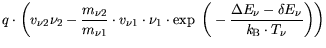
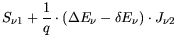
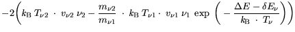
relations for the current density  and energy fluxes
 across the interface read:
 |
 |
 |
(3.87) |
|
|
 |
(3.88) |
 |
|
 |
(3.89) |
|
|
 |
(3.90) |
 with
with  = n,p represents the effective
masses at both sides of the interface between the segments i=1
and i=2, respectively.
= n,p represents the effective
masses at both sides of the interface between the segments i=1
and i=2, respectively.
 represents the conduction
or valence band discontinuity. The effective barrier reduction
represents the conduction
or valence band discontinuity. The effective barrier reduction
 is modeled as function of the electric field
 orthogonal to the interface.
| |
|
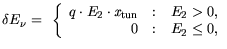 |
(3.91) |
A fit of the barrier reduction
for the
Al Ga
Ga As/In
As/In Ga
Ga As interface was
performed in [50] and extended to different material
systems, such as AlGaAs/GaAs, InAlAs/ InGaAs, and AlGaN/GaN. The
tunneling parameters are found in Table 3.33. These are
effective fitting parameters, however, they scale with the
tunneling probabilities found in Appendix B.
As interface was
performed in [50] and extended to different material
systems, such as AlGaAs/GaAs, InAlAs/ InGaAs, and AlGaN/GaN. The
tunneling parameters are found in Table 3.33. These are
effective fitting parameters, however, they scale with the
tunneling probabilities found in Appendix B.
Table 3.33:
Tunneling parameters for various materials.
| Material |
Material Composition |
 |
| |
 |
[nm] |
| AlGaAs/GaAs |
- |
3 |
| AlAlAs/InGaAs |
- |
7 |
In Al Al As/In As/In Ga Ga As As |
- |
8 |
In Al Al As/InGaAs As/InGaAs |
0.33  x 0.66 x 0.66 |
7-8 |
| AlGaN/GaN |
0.25 |
3 |
|
The thermionic field emission velocity for the segment i
is defined as follows:
| |
|
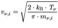 |
(3.92) |
The thermal boundary condition between semiconductors
in general reads as follows:
| |
|
 |
(3.93) |
In the case of heterointerfaces additional entries are necessary in the DD simulation to
account for the carriers loosing or gaining energy.
| |
|
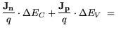 div div |
(3.94) |
For the HD case this is not required, since the energy relations
yield this condition self-consistently.
Next: 3.3.2 Semiconductor-Insulator Interfaces
Up: 3.3.1 Semiconductor-Semiconductor Interfaces
Previous: 3.3.1.1 Continuous Quasi-Fermi Level
Quay
2001-12-21