


Next: 3.3.5 Boundaries
Up: 3.3.4 Semiconductor-Metal Interfaces: The
Previous: 3.3.4.2 The Ohmic Contact:
For the gate contact in the HEMT two models are commonly used to model
the Schottky contact. The first model for the contact interface
condition for the potential is:
| |
|
 |
(3.111) |
where:
| |
|
 |
(3.112) |
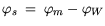
Thus, the potential at the boundary in the semiconductor
 is set to the difference of the quasi-Fermi level potential in
the metal
is set to the difference of the quasi-Fermi level potential in
the metal  , which is equal to the potential specified at the contact, and
the potential
, which is equal to the potential specified at the contact, and
the potential
 . The latter represents the potential
corresponding to the work function difference energy
. The latter represents the potential
corresponding to the work function difference energy  of metal and semiconductor.
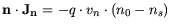
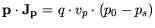
The applied current equations are:
of metal and semiconductor.
The applied current equations are:
| |
|
 |
(3.113) |
| |
|
 |
(3.114) |
The currents are proportional to the so-called
recombination velocities  and the difference of the
carrier concentration
and the difference of the
carrier concentration  and
and  . The carrier concentrations at the
boundary read:
. The carrier concentrations at the
boundary read:
| |
|
 |
(3.115) |
| |
|
 |
(3.116) |
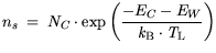
while the equilibrium concentrations  and
and  can be expressed as:
| |
|
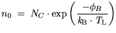 |
(3.117) |
| |
|
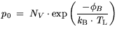 |
(3.118) |
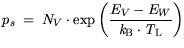
For the Schottky barrier height  typical values range between 0.61 eV and 0.8 eV.
For the hydrodynamic case the carrier temperatures are fixed, thus thermal equilibrium is assumed
similarly to the Ohmic contact. The thermal boundary conditions
applied similar to the Ohmic contact, i.e. either by an thermal resistance or a isothermal boundary condition.
The model presented so far can also be called a thermionic emission model:
The recombination velocity in (3.113) is then to be called a thermionic emission
velocity. Inserting (3.115) and (3.117) into (3.113) we obtain:
typical values range between 0.61 eV and 0.8 eV.
For the hydrodynamic case the carrier temperatures are fixed, thus thermal equilibrium is assumed
similarly to the Ohmic contact. The thermal boundary conditions
applied similar to the Ohmic contact, i.e. either by an thermal resistance or a isothermal boundary condition.
The model presented so far can also be called a thermionic emission model:
The recombination velocity in (3.113) is then to be called a thermionic emission
velocity. Inserting (3.115) and (3.117) into (3.113) we obtain:
| |
|
![$\displaystyle \mathbf{n}\cdot\mathbf{J_n} = - q \cdot v_s \cdot N_C \bigg[ \exp...
...igg(\frac{-E_C-E_{W}}{{\it k}_{\mathrm{B}}\cdot {\it T}_\mathrm{L}}\bigg)\bigg]$](img640.gif) |
(3.119) |
As stated by Schroeder in [249],
(3.119) can thus be written as:
| |
|
![$\displaystyle \mathbf{n}\cdot\mathbf{J_n} = \frac{q \cdot m_n {\it k}_{\mathrm{...
...-\frac{ E_{Fm}-E_{Fsemi}}{{\it k}_{\mathrm{B}}{\it T}_\mathrm{L}}\bigg)-1\bigg]$](img641.gif) |
(3.120) |
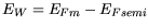
using =  -
-  which is already named the Schottky barrier height.
Furthermore we use:
which is already named the Schottky barrier height.
Furthermore we use:
| |
|
 |
(3.121) |
which says that the work function difference is equal to the difference of the Fermi levels
of the semiconductor and the metal.
The velocity  is rewritten as (see (3.92)):
| |
|
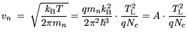 |
(3.122) |
where A is the Richardson constant typical for thermionic emission processes.
Thus, (3.122) represents a typical thermionic emission equation, which is determined by the Schottky barrier
height and the difference of the Fermi levels. Neglecting the tunneling in (3.91) the similarities are obvious.
Typically the Fermi level of the semiconductor is chosen as the reference energy.
A second model for the metal semiconductor interface including a tunneling current component has been tested [130,174].
It is based of the equivalence of a tunneling current and a generation process. It was found that such a non-local model is physically sound
and useful on the first glance, but its usefulness depends critically on the actual two-dimensional implementation of the integration path for the tunneling probability
in general purpose simulators, as stated in Section 3.6.
Next: 3.3.5 Boundaries
Up: 3.3.4 Semiconductor-Metal Interfaces: The
Previous: 3.3.4.2 The Ohmic Contact:
Quay
2001-12-21