Next: 1.1.2 Shrinking Features Up: 1.1 Integration Technology Previous: 1.1 Integration Technology
The individual components of an IC are extremely small and its production demands precision at an atomic level [117]. IC fabrication is a complex process during which electronic circuits are created in and on a wafer made out of very pure semiconducting material, typically silicon. The manufacturing is a multiple-step sequence which can be divided into two major processing stages, namely front-end-of-line (FEOL) processing and back-end-of-line (BEOL) processing.
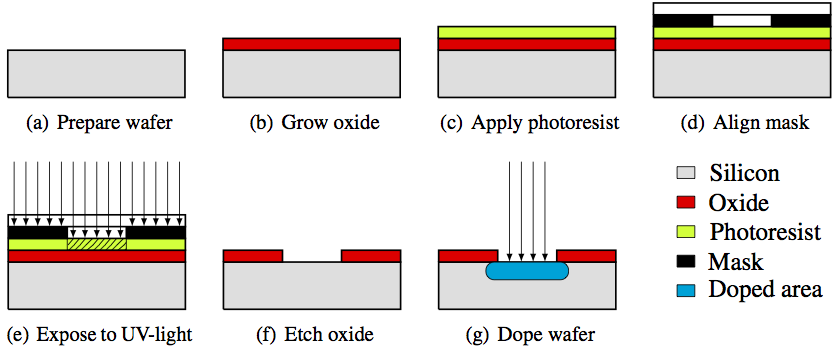
FEOL refers to the construction of the components of the IC directly inside the wafer [5], as depicted in 1.1. The mono-crystal silicon wafer is polished in order to obtain a substrate with its surface as regular and flat as possible (1.1a). The top of the wafer is then prepared for photolithography by covering it with an insulating layer to serve as a mask, typically an oxide (1.1b), and a subsequent covering film of protective material which is sensitive to light, called photoresist (1.1c). A photomask with the circuit pattern for one layer of the chip is loaded and aligned with the wafer (1.1d). The exposure process of the wafer to intense UV light through the mask allows to remove the exposed photoresist area (1.1e). The unprotected insulating material is then striped away using a chemical etching process and the remaining photoresist is removed by a developer solution (1.1f). In general, there are two types of photoresist: negative and positive. When exposed to UV light, the negative photoresist becomes polymerized and more difficult to dissolve in developer solution than the positive resist. For negative resist, the developer solution removes only the unexposed areas. In this way, it is possible to create a pattern of non-protected silicon wafer areas surrounded by regions of non-conducting material. Then, the modification of the electrical properties of the exposed areas involves doping processes, such as ion implantation which is used to create sources and drains of the transistor (1.1g). Other conducting or insulating layers may also be added. A new layer of material is added and the entire photolithography process, which includes imaging, deposition, etching, and doping, is repeated to create many different components of the chip, layer by layer.
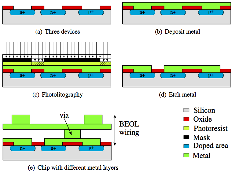
Once all the components of the IC are ready, the BEOL processing step is performed to deposit the metal wiring between the individual devices in order to interconnect them, with a process called metallization [5], as illustrated in 1.2. Common metals used in the semiconductor industry are copper and aluminum, but recently many other metals are being tested for applicability for metal interconnects at the nano-scale. The second stage of the chip fabrication also includes the formation of contacts and dielectric structures. BEOL processing generally begins when the first layer of a conducting metal is deposited on top of the wafer (1.2b). A layer of UV-sensitive photoresist is added on the top of the metal. Then, in a manner similar to the processing of the components during the FEOL processing, a UV-light source is exposed to the photoresist through a mask describing the desired layout of the metal wires; the exposed section of the positive photoresist is then removed in the subsequent chemical etching step (1.2c). The etching process eliminates the unprotected metal to obtain a pattern of wires described by the mask which connects the different components of the chip (1.2d). Most ICs need more than one layer of wires to form all the necessary connections. In real chips, as many as 5-12 layers are added in the BEOL process [117]. Typically, metal interconnecting wires are isolated by dielectric layers to prevent the wires from creating a short circuit with other metal layers. The various metal layers are interconnected by etching holes, called vias, in the insulating material (1.2e).
After the BEOL processing, the post-fab process is performed, which includes wafer testing, die separation, die testing, IC packaging, and final device testing.