Next: 1.1.3 Interconnects in Integrated Circuits Up: 1.1 Integration Technology Previous: 1.1.1 Semiconductor Fabrication
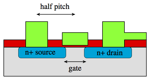
Today, ICs can be made very compact and the most advanced ICs can contain several billions of electrical components on an area of about 1cm [6]. The density of individual components which can be electrically connected in an IC is related to the device half-pitch [2]. It represents the half of the distance between the parallel conducting metal lines at the first metallization level which carry the electrons to the chip, as depicted in 1.3. It is an important feature in the semiconductor industry because, with the shrinking of the ICs, other terms, such as node and gate width, resulted no more universally accepted metrics that specialists use to measure their transistors due to the continued reduction of their sizes [2]. A node indicates the size of the smallest part of the transistor on the chip, while the gate width is the distance between the source and the drain of the transistor. For example, in 2005, the node on an Intel microprocessor was 65nm, the gate width was 32nm, but the half pitch was 105nm [2]. Therefore, since the half pitch was becoming bigger than the node and gate width, these concepts were no longer meaningful descriptors of the evolution of the miniaturized chip fabrication lines. The average device half-pitch on chips became smaller and smaller as the technology advanced, reducing to around 14nm in 2014 [83].
 |
This shrinking trend of the feature size of the chip over the years is commonly related to Moore's Law. In 1965 Gordon Moore, the co-founder of Intel, predicted that the number of components of a dense IC will double every year [114]. The forecast was extended to eighteen months to accommodate real conditions in 1975 [113]. As the technology progressed, the number of components contained on a single chip has been increased from 10 in 1964 to several billions in the 1980s. This led to the classification of different generations of ICs, giving rise to new design methods from the early small-scale integration (SSI) to the more complex ultra-large-scale integration (ULSI) and three-dimensional integrated circuit (3D-IC). The key technology of the development reflects on the further evolution in the complexity of ICs by building systems in which all the individual components are assembled in circuit blocks, such as memory and logic, and included in a single chip substrate.
Moore's prediction was an elegant statement of how ICs would become smaller and cheaper over the years. The law has been used in the semiconductor industry to set targets for product development for several decades and represents a technological driving force for social change and economic growth [89]. The fascinating technology evolution was essentially supported by the maturation of the chip fabrication process, but physical limitations of device shrinking were starting to affect IC performance and reliability [122].