Next: 5.1.3 Void Growth Analysis Up: 5.1 Electromigration Failure in Open TSVs Previous: 5.1.1 TSV Design and Simulation Parameters
In open TSV technologies, the fabrication process induces imperfections and the severe mismatch of geometric features between metallic layers at the TSV bottom can lead to the
nucleation of a small void under the TSV, initiating the electromigration failure mechanism.
Voids nucleate especially at those locations in the structure where the adhesion between the copper line and the surrounding layer is weak.
These sites are generally observed close to the metallization barrier between the TSV and the adjacent metal film [61].
The identification of void nucleation sites in a typical passivated metal line is related to the primary material transport path along which electromigration acts, namely the fast diffusivity
path, which is recognized to be the surface of the nucleated void close to the metal/barrier interface [40].
Consequently, material interfaces, in addition to the void surface, play a key role when it comes to understanding the mechanism by which electromigration failure progresses in interconnects.
Vacancy Accumulation at the TSV Bottom
The copper film in the TSV structure is surrounded by titanium nitride layer (barrier) at the bottom and by silicon dioxide layer (capping) at the sides. These interfaces act as blocking boundaries for the electromigration vacancy flux causing accumulation of vacancies at these interfaces. As discussed in Section 3.2, the vacancy dynamics model describes the local change of vacancy concentration in time due to the contribution of the vacancy transport as well as the generation/annihilation processes inside the fast diffusivity path, as presented in equation (3.26). In (5.2), three distinctive stages of the time evolution of the maximum relative vacancy concentration are recognizable. These stages are explained according to [91] and can be related to the impact of the different driving forces governing the vacancy flux Jv associated with equation (3.24).
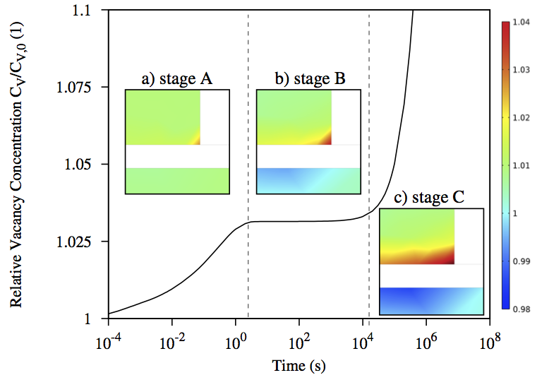 |
In the first stage (A), the transport of vacancies is dominated by the flux induced by the electromigration driving force. The reaction of the material in this stage, due to the gradients of the stress and the vacancy concentration, is considerably smaller than the electromigration itself. As a result vacancies tend to accumulate close to the interface region between copper and titanium nitride ((5.2(a))). After about 1s the vacancy concentration reaches a quasi-steady state (stage B). During this stage, the response of the material tends to perfectly balance electromigration ((5.2(b))). The quasi-steady state is followed by a rapid growth of the vacancy concentration (stage C) caused by stress-activated vacancy sources ((5.2(c))). During this stage, the source/sink term in equation (3.26), which models vacancy generation/annihilation processes, leads to a higher accumulation of vacancies close to the interface region which results in a rapid development of stress in the structure. The flux induced by the stress gradient is the dominant term of the vacancy flux equation (3.24) during this stage.
As presented in Section 2.5.2 Korhonen et al. [93] derived a model which provides the time evolution of the stress build-up during the three phases of the vacancy dynamics, observed in (5.2). During the first two phases the maximum stress exhibits linear growth with time, as depicted in (2.3). After a certain time the stress increases with the square root of time, until reaching a threshold value. In the following, the reasons for the stress development in the structure and the idea behind why reaching a certain threshold value is considered a requirement for electromigration void nucleation will be explained.
By monitoring the distribution of the hydrostatic stress in the TSV structure (5.3), the locations with the highest probability of void formation are identified. Void nucleation mainly occurs in those locations where vacancies accumulate. In the case study, the site of vacancy accumulation is at the TSV bottom, where the TSV intersect the capping and the barrier layers. Due to the slight relaxation of the lattice surrounding a vacancy, vacancy accumulation produces a volume contraction of the structure resulting in the development of tensile stress in these areas. Here, the tensile stress increases from the periphery, which is closed to the interface, towards the interface regions of the copper and titanium nitride. In turn, at the specular interface sides, a compressive stress is observed due to the volume expansion of the structure produced by vacancy depletion.
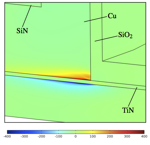 |
Therefore, the Cu/TiN/SiO2 corner intersection is identified as the location with the highest probability of void formation in the open copper TSV structure. It has been experimentally shown that this is the typical site for void nucleation in copper dual-damascene structures with TSVs mainly due to the lower cohesive energies of the surrounding layers and fabrication defects [61].
In order to estimate the void nucleation time, the stress distribution at such sites in the structure is monitored by an increase of the current density by 30%. From the simulation results, the time evolution of the stress build-up due to electromigration is obtained for a total of four current densities ((5.4)).
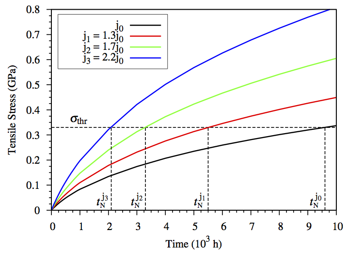 |
As expected [93], the maximum tensile stress increases with the square root of time, until it reaches the threshold value for void initiation. Following equation (3.72) [63] and assuming an initial adhesion-free patch Rp of 10nm, an interfacial free energy of copper γCu of 1.65N/m, and a critical contact angle θc of 90°, the threshold stress σthr calculated for the particular case study is 0.33GPa. The electromigration void nucleation time te for a given applied current density is determined as the time needed to reach this limit. Applying lower current densities means that a longer time is needed to reach the threshold stress for void nucleation. Furthermore, it should be noted that during this time period the TSV resistance does not change. The void has been nucleated and its small size is not able to produce a significant increase of the electrical interconnect resistance.