Next: 5.1.4 Lifetime Estimation Up: 5.1 Electromigration Failure in Open TSVs Previous: 5.1.2 Void Nucleation Analysis
Once the location of void nucleation in the interconnect structure is identified, electromigration-induced proceeds and failure is ultimately caused by the growth of the fatal void.
As discussed in Chapter 3, the mechanism of void growth due to electromigration is mainly related to surface diffusion during this phase of failure.
Atoms are transported to the void surface and diffuse along it until they reach the material interface.
The responsible driving forces are the electric current flow, the stress gradient, and the surface curvature gradient.
The diffusion of atoms along the void surface causes it to change its shape resulting in the void growth.
Another small contribution governing the void growth is represented by feeding the void with vacancies coming from the bulk.
The evolution of voids due to electromigration-induced surface diffusion can be modeled by employing two different methodologies, namely diffuse interface and semi-empirical models, as
discussed in Chapter 3.
In the following, both methods will be applied to study the void evolution mechanism in the open TSV structure under accelerated test conditions of increased temperature and current density.
Diffuse Interface Model
The diffuse interface model is employed to simulate the dynamics of pre-existing voids in open TSVs. In order to investigate the resistance change due to the void evolution dynamics in an open TSV structure, a 2D diffuse interface model is constructed to describe the void growth caused by vacancy accumulation near the Cu/TiN interface at the TSV bottom. The configuration considered in the diffuse interface calculations is illustrated in the highlighted area in (5.5(a)).
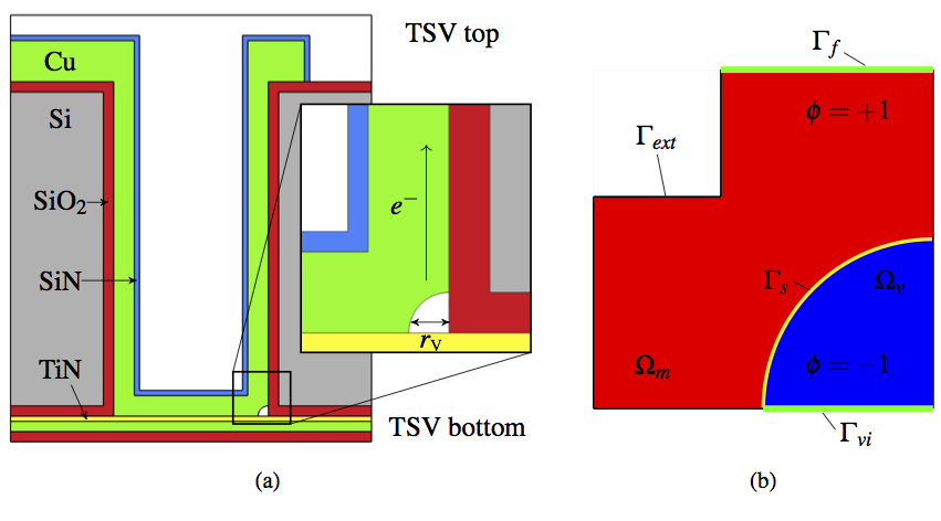 |
The portion of the open copper TSV structure analyzed is represented geometrically as a copper interconnect surrounded by passivation (SiN), insulation (SiO2), and barrier (TiN) layers. The outer material interfaces surrounding the copper line are taken to be rigid. A small void is placed at the site of void nucleation within the metallization (Cu/TiN interface) with its surface free to move. The initial void radius rv is assumed to be 10nm. Since copper is much more susceptible to electromigration than titanium nitride, the flux of vacancies is considered only in the copper line of the structure depicted in (5.5(a)). The computation of the order parameter field is therefore only restricted to the copper domain of the structure, as illustrated in (5.5(b)). Since the analysis is restricted to a 2D portion of the copper domain which contains a quarter of a circular void extending throughout the width of the interconnect line, the case study reduces to an unpassivated metal line. This approximation leads one to neglect the effect of mechanical stress in the unconfined line. This also allows to neglect the effects of grain boundaries and lattice diffusion, because diffusion at the void surface is considered to be much faster than in the bulk and the grain boundaries [62]. Furthermore, the study is restricted to the case of an isotropic medium.
The setting of the initial values for the order parameter in the domain serves as an initial condition for the simulation. The initial value of the order parameter in the void region Ωv of the domain is indicated with φ=-1 (blue region in (5.5(b))), while the initial order parameter value in the bulk material Ωm is defined with φ=+1 (red region in (5.5(b))). The initial position of the metal-void interface Γs is therefore represented with the value φ=0 (yellow line in (5.5(b))). No-flux boundary conditions (3.83) are applied to the external surfaces of the domain. If no-flux boundary conditions are established at all external boundaries, the void modeled by the solution φ of the Cahn-Hilliard equation (3.82) does not grow, but keeps its volume constant in time. In order to predict the growth of the void, when it is on the edge of the domain, the Cahn-Hilliard equation should be extended with a source term which allows the creation of the order parameter. For this purpose, Dirichlet boundary conditions are applied at the boundaries Γf and Γvi of the domain (thick green lines in (5.5(b))). Dirichlet and no-flux boundary conditions related to the case study can be summarized as follows
where Vf is the volume fraction of the material and void phases. A value Vf=1 specifies the solution φ along the Γf boundary at the lower side of the metal phase, while a value Vf=0 represents the order parameter at the Γvi boundary representing the Cu/TiN interface of the void phase. The source term allows for the creation of the order parameter and, consequently, allows for the void to expand. No-flux boundary conditions are applied to the other boundaries Γext of the domain (black lines in (5.5(b))) in order to maintain the conservation of total mass. Operating conditions for electromigration simulations are set by imposing boundary conditions over appropriate regions of the case studied. All external surfaces of the structure are assumed isotherm. For electrical loading, the lower side of the copper line is maintained at j0=1MA/cm2, and the Cu/TiN interface is set as ground. The Cu/TiN interface acts as an electromigration blocking boundary and prevents the void from propagating into the barrier layer while current flows through the copper line. The configuration presented in (5.5) represents the starting point of the FEM simulation, where resistance increase due to the growth and evolution of a void at the TSV bottom is investigated by employing the diffuse interface method.
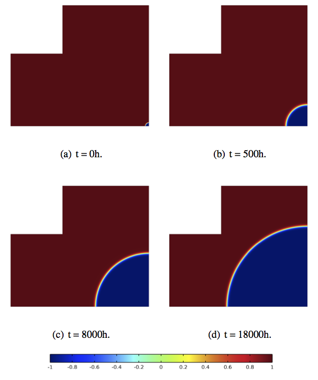 |
(5.6(a)) shows the position of the initial void in the interconnect. Since higher electromigration-induced stress levels are observed at the TSV bottom close to the Cu/TiN interface, as discussed in the previous section, the initial void is placed at the corner of the copper, barrier, and insulation layers. Within the structure, the void begins to grow due to electromigration and moves in the same direction as the electron flow. After some time, the void gradually increases in size as illustrated in (5.6(b)) and (5.6(c)). The choice of the no-flux boundary conditions together with the Dirichlet boundary conditions, at the prescribed boundaries of the domain presented above, for the solution of the Cahn-Hilliard equation (3.82) allows for the simulation growth of the void caused by the action of the electromigration force. The creation of the order parameter at these boundaries enforces the non-conservation of the order parameter in the domain and allows for the change of the void's area in time. Without these boundary conditions, the void would not grow, but would instead keep its area constant in time because of the conservation of the total mass of the bulk material. In real interconnects, the void is not conserved and its evolution is related to the fact that the electric current flow drives the vacancies towards the Cu/TiN interface, where they are captured at the void surface. In turn, at the opposite side, the increased atom flux would generate a hillock. Vacancies may diffuse along the void surface causing it to change its shape and leading to the void growth [62]. In addition, the surface minimizing diffusion term tends to maintain a stable circular shape throughout the growth process. Then, the void spreads across the full width of the metal-barrier interface leading to open circuit failure (5.6(d)). This evolution of the void influences the conducting metal cross section and therefore affects the interconnect resistance. Since diffusion on the void surface is assumed to be isotropic, the void has a rounded morphology and remains rounded throughout its evolution.
Another method used to simulate the growth of the void in the open copper TSV structure is based on a semi-empirical approach, as described in Section 3.4.3. The semi-empirical method assumes that the volumetric growth of the void is due to changes in the vacancy concentration distribution on the void surface driven by the electron wind force. The growing void depends on the rate at which vacancies reach the void and transport along its surface, caused by changes in the current density around the void itself. The rate of vacancy transport along the surface is therefore mainly due to electromigration and is taken to be proportional to the tangential component of the current density at the surface, as mentioned in Section 3.4.2.
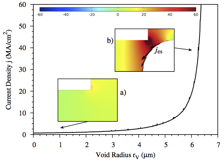 |
By following the modeling approach described in Section 3.4.3, an initial spherical void of radius rv=10nm is placed at the location of void nucleation and its radius is increased ((5.5(a))). (5.7) shows the current density distribution close to the void nucleation location for different void sizes in the simulated structure. Electron flow leads to current crowding at the TSV bottom, towards the corner, where the void, copper, and barrier layers meet, even if the radius of the void is small in size ((5.7(a))). Current crowding arises especially at the TSV bottom close to the sites of void nucleation because of the diverse layers' varying geometries and electrical conductivity properties. The current flow tends to feed the void surface with vacancies, implying vacancy transport along it and consequently increasing the volume of the void. As soon as the void becomes larger, current density divergences are more prominent around the void surface, as shown in (5.7(b)). The average current density over the void surface can be monitored at every point along the surface itself. (5.7(b)) shows that the main driving force affecting the diffusion of vacancies along the void surface is observed to be proportional to the tangential component of the current density to the surface. Peak values of jes are located at the metal-void interface, where current crowding is higher. This is in good agreement with the simulation results obtained by means of FEM simulations using a diffuse interface approach in [28]. The electromigration driving force causes significant void growth as the void propagates through the line. The growing void reduces the effective TSV conducting area at the bottom of the TSV, leading to higher current crowding in these regions.
Under these circumstances it is obvious that as the line nears complete failure, the resistance of the interconnect increases non-linearly with time. The resistance change with time is associated to the growth of the void located at the Cu/TiN/SiO2 intersection at the TSV bottom. The open TSV fails after the maximum tolerable resistance level is exceeded, typically a resistance increase of 20%. The electromigration void evolution time te is determined as the time needed to reach the maximum tolerable resistance value. The determination of the resistance/time curves is based on the simulation results regarding the growth of the void obtained from the two different approaches described above under different stress conditions of current density, as illustrated in (5.8). The resistance increase of the given interconnect is monitored by increasing the initial current loading by 30%. In this way, it is possible to extract the different void evolution times.
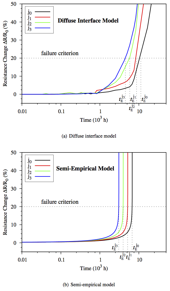 |
Numerical solutions equations (3.85)-(3.88), together with the solution of the Cahn-Hilliard equation (3.82), allows one to determine the change in the interconnect resistance during void evolution by following the diffuse interface method. At each time step, it is possible to extract the position of the void and the interconnect resistance from the computation of the order parameter and from the numerical solution of the electrical problem, respectively. In this way, the change in interconnect resistance throughout the entirety of void growth is obtained, as depicted in (5.8(a)). In addition, increasing the applied current density results in a decrease in the time required to reach the failure criterion. Here, an increase in the resistance is accelerated due to a more intense electromigration flux induced by higher current densities.
In a similar way, the resistance/time curves during the void evolution period are obtained by following a semi-empirical approach, as depicted in (5.8(b)). The numerical simulation results for the vacancy flux captured by the void surface which produces changes in the current density and vacancy concentration distribution are inserted into equation (3.94). By performing a numerical integration, it is possible to obtain the time necessary to grow a void of a given volume. Furthermore, numerical solutions of the electrical problem (Section 3.1) allow to determine the interconnect resistance change during the void evolution period. In this way a relationship between the open copper TSV resistance and time for different initial electrical loadings can be observed, as plotted in (5.8(b)).