


Next: 8.1.2 Device Characterization
Up: 8.1 An Optimization Scenario
Previous: 8.1 An Optimization Scenario
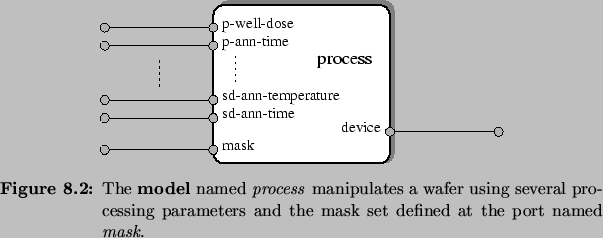
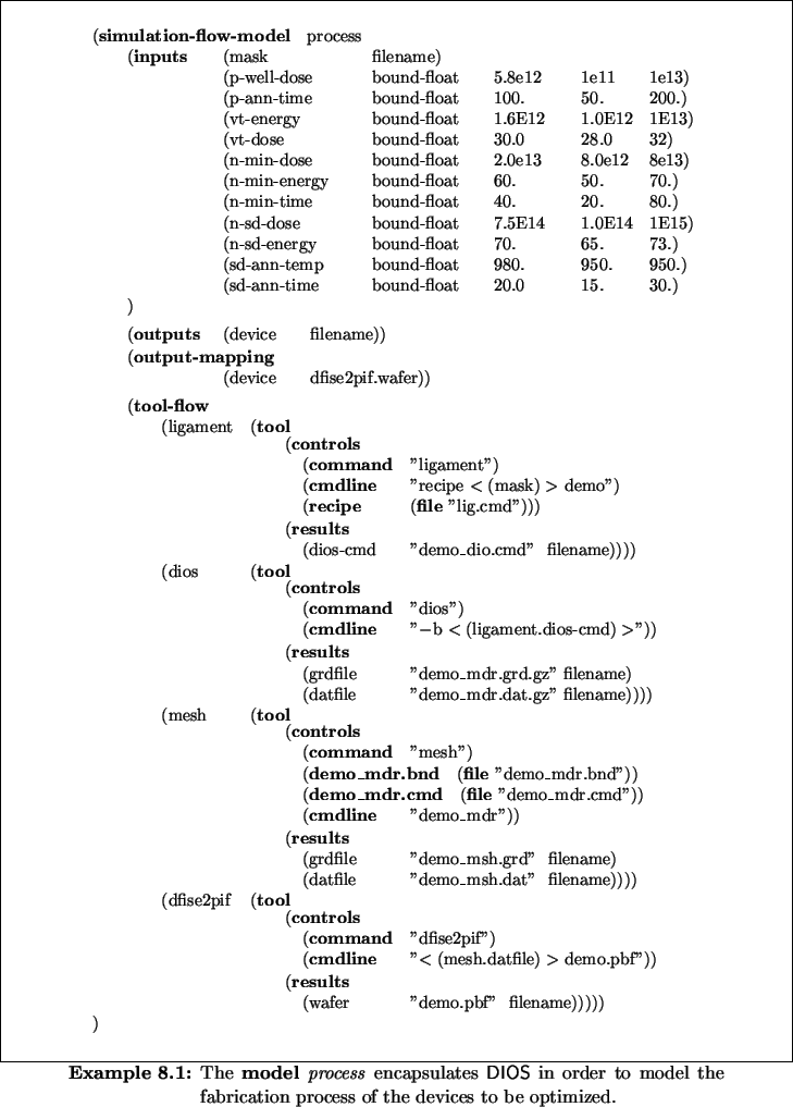
In order to model the fabrication process we use a simulation-flow-model
named process (Example 8.1,
Figure 8.2) which encapsulates the
DIOS [37] process simulator. It has input ports representing
several processing parameters of fabrication steps, and one port
(mask) which allows the specification of the mask set which
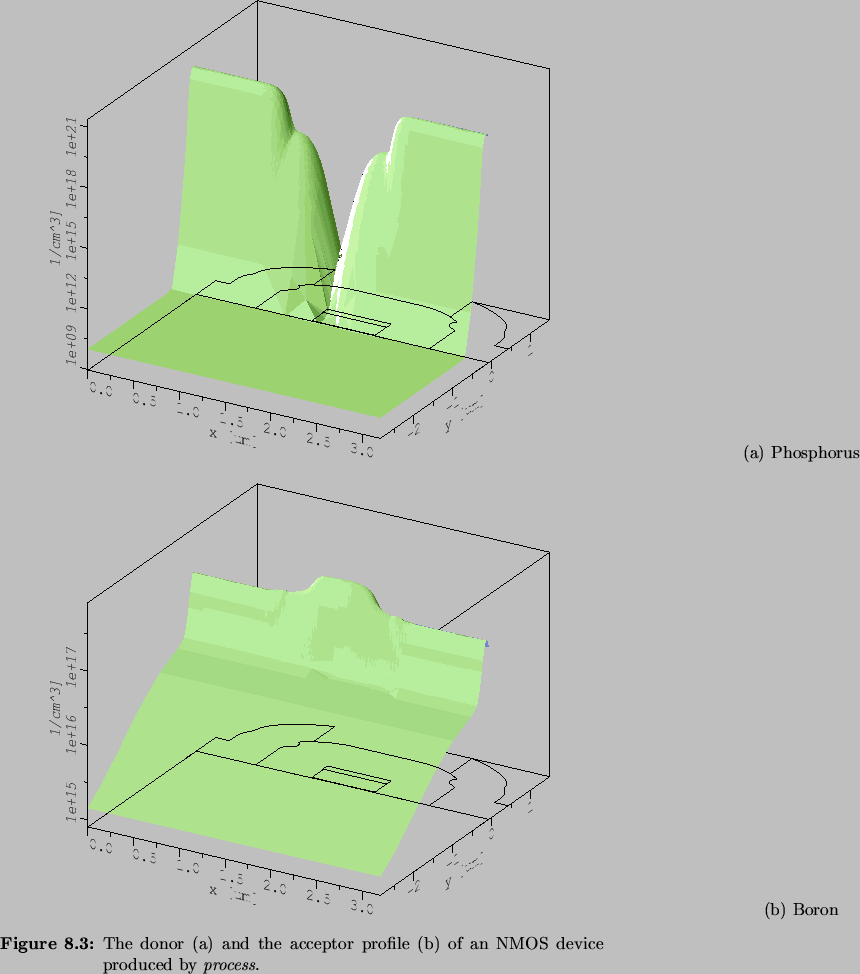
is used during fabrication. The wafer description produced by DIOS
is processed by the MESH [38] gridding utility in order
to create a mesh which is suitable for device simulation at a later
stage. Since we want a PIF device description as the result of this
model, it is necessary to introduce a conversion
tool (dfise2pif) for this purpose. Figure 8.3
depicts an example of a device produced by process.
Rudi Strasser
1999-05-27