


Next: 8.1.2.1 Simulator Initialization
Up: 8.1 An Optimization Scenario
Previous: 8.1.1 Modeling the Fabrication
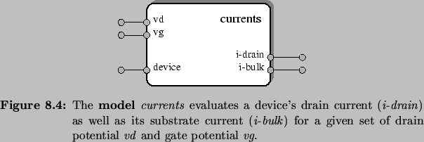
The electrical modeling of the devices is performed using
MINIMOS-NT. Figure 8.4 shows the currents model which is
used for this purpose (see also Example 8.2). It allows
the specification of the drain and the gate potential at its input
ports vd and vg, respectively. By specifying
different values at these ports, the implementation of the
currents model can be multiply used for the modeling of the drive
current, the substrate current, and the leakage current.
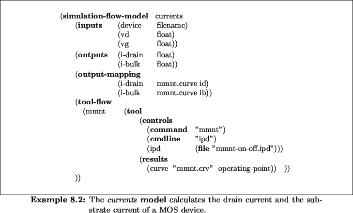
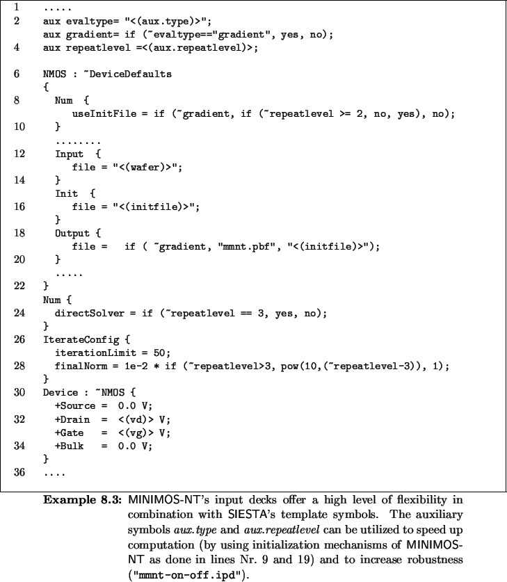
Example 8.3 shows the input deck template which is used to
control MINIMOS-NT within the simulation-flow-model shown in
Example 8.2. Among other template symbols it includes
symbols named vd, vg, and device which
define the potential at the drain contact, the potential at the gate
contact of the device, and the device description, respectively. The
values of these symbols will be inserted into the input when SIESTA
evaluates this model. Additionally, there are parameters named
aux.repeatlevel, aux.type, and
aux.initfile.
Next: 8.1.2.1 Simulator Initialization
Up: 8.1 An Optimization Scenario
Previous: 8.1.1 Modeling the Fabrication
Rudi Strasser
1999-05-27