The input data to the model
, i.e., terminal currents and charges for a set of terminal voltages,
can be obtained either by measurements
or by process and device simulations. In this work we used VISTA
with MINIMOS [54] to obtain the device data by simulation.
All conductive currents can be obtained directly from DC measurements.
The charge data are computed from transient simulations as shown in
Fig. 4.1 for the case of a two-pole: the device is modeled
as a quasi static black box which is equivalent to a non-linear
conductance parallel to a non-linear capacitance
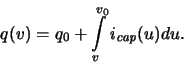
C(v)=dq/dv. Applying a symmetric trapezoidal voltage v(t) to the
device will result in a current i(t) which can be separated into a
conductive and a capacitive component,
![$\displaystyle \frac{1}{2}\left[ i(t_1(v))+i(t_2(v)) \right],$](img507.gif) |
(4.1) | ||
![$\displaystyle \frac{1}{2}\left[ i(t_1(v))-i(t_2(v)) \right],$](img509.gif) |
(4.2) |
![\includegraphics[scale=1.2]{tr2iq.ps}](img512.gif)
|
To obtain a complete field of charge data, including the charge
offset, a series of transient measurements/simulations is required
as shown in Fig. 4.3.
According to the desired ranges and step sizes of
![]() ,
,
![]() ,
and
,
and
![]() ,
one transient in
``
,
one transient in
``
![]() -direction'', n transients in ``
-direction'', n transients in ``
![]() -direction'', and n x m
transients in ``
-direction'', and n x m
transients in ``
![]() -direction'' are measured or simulated.
The simulations in ``
-direction'' are measured or simulated.
The simulations in ``
![]() -direction'' yield the main data set
which is used for i/q extraction.
The simulations in ``
-direction'' yield the main data set
which is used for i/q extraction.
The simulations in ``
![]() -direction'' and ``
-direction'' and ``
![]() -direction''
are required for the charge offset computation.
The steepness of the ramp determines the accuracy of the charge data
and the influence of non-stationary effects accordingly. Both can be
verified with single transient measurements, using the
i/q-extraction software.
For the simulation with MINIMOS the input decks are generated
automatically according to the range settings which also control
the computation of the current/charge data.
Figure 4.4 shows a comparison with gate capacitance data obtained
from accurate gate charge simulations using MINIMOS.
-direction''
are required for the charge offset computation.
The steepness of the ramp determines the accuracy of the charge data
and the influence of non-stationary effects accordingly. Both can be
verified with single transient measurements, using the
i/q-extraction software.
For the simulation with MINIMOS the input decks are generated
automatically according to the range settings which also control
the computation of the current/charge data.
Figure 4.4 shows a comparison with gate capacitance data obtained
from accurate gate charge simulations using MINIMOS.
![\includegraphics[scale=1.0]{tr.eps}](img517.gif)
![\includegraphics[scale=1.0]{iq-q.eps}](img518.gif)
|
![\includegraphics[scale=1.0]{cg-vg.eps}](img523.gif)
![\includegraphics[scale=1.0]{cg-vd.eps}](img524.gif)
|
![\includegraphics[scale=1.41]{trmos.ps}](img521.gif)
![\includegraphics[scale=1.20]{stimul.ps}](img522.gif)