


Next: 5.2.2 Switched-Capacitor Resistors
Up: 5.2 Switched-Capacitor Circuits
Previous: 5.2 Switched-Capacitor Circuits
5.2.1 Analog Switches
Analog switches can be implemented just like digital switches,
i.e., as individual transistors or, if the full voltage range is
required, as transmission gates.
Although transmission gates for digital applications work well for
low supply voltages, the situation is more complex in analog circuits.
Especially in switched-capacitor circuits a number of problems can
arise:
- 1.
- Both on-state and off-state resistance of the switch depend critically
on the terminal voltages of the switch. Especially, the off-state
resistance
which is limited by the transistors' drain conductance
decreases exponentially as the analog signal approaches ground or
 .
.
- 2.
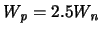
- In order to compensate the charge injection from the transistors
the PMOS transistor should not be larger than the NMOS transistor.
In order to achieve a symmetric and low turn-on resistance the PMOS
transistor should be twice as wide.
To use dummy NMOS transistors at either terminal of the switch may
be too much overhead.
- 3.
- Leakage currents in fast switches (i.e.,
 ), which may be
still acceptable for dynamic digital circuits, can be much too
high for some analog applications because of the lack of signal
regeneration in linear analog circuits.
), which may be
still acceptable for dynamic digital circuits, can be much too
high for some analog applications because of the lack of signal
regeneration in linear analog circuits.
- 4.
- When constant-field technology scaling is assumed for
switched-capacitor circuits, a down-scaling by
 means a reduction of the capacitances and voltages by
.
This means that the signal power
means a reduction of the capacitances and voltages by
.
This means that the signal power
 scales as
 and the thermal kT/C noise scales as
 .
Thus, the SNR is reduced by
.
Thus, the SNR is reduced by
 .
.
Figure 5.7:
Low-voltage analog transmission gate switch
(
 ,
,
 )
)
![\includegraphics[scale=1.0]{swtch-1.eps}](img590.gif)
|
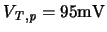
Figure 5.8:
Low-voltage analog transmission gate switch
(
 ,
)
,
)
![\includegraphics[scale=1.0]{swtch-2.eps}](img593.gif)
|
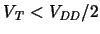
Simulation results of low-voltage analog switches in a
 ULP CMOS technology are shown in
Figs. 5.7 and 5.8:
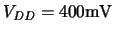
Fig. 5.7 shows the resistance curves of a
transmission gate switch with
operating
at
(the threshold voltages are
ULP CMOS technology are shown in
Figs. 5.7 and 5.8:
Fig. 5.7 shows the resistance curves of a
transmission gate switch with
operating
at
(the threshold voltages are
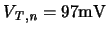 and
and
 ).
The circuit exhibits a fairly low, almost symmetric
on-state resistance.
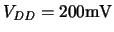
Fig. 5.8 shows the same circuit at the half supply voltage
(
).
The circuit exhibits a fairly low, almost symmetric
on-state resistance.
Fig. 5.8 shows the same circuit at the half supply voltage
(
 ),
where the on-state conductance and off-state resistance are reduced.
Nevertheless, the switch still works properly, albeit with somewhat
degraded properties.
),
where the on-state conductance and off-state resistance are reduced.
Nevertheless, the switch still works properly, albeit with somewhat
degraded properties.
Next: 5.2.2 Switched-Capacitor Resistors
Up: 5.2 Switched-Capacitor Circuits
Previous: 5.2 Switched-Capacitor Circuits
G. Schrom