One important class of CMOS analog integrated circuits are
switched-capacitor (SC) circuits, where high-precision
resistors with large resistance values
are implemented by switches and capacitors [28].
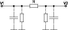
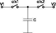
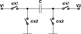
Figure 5.9 shows implementations of a switched-capacitor resistor
and the equivalent circuit. Ideally, the equivalent resistance is
|
[Equivalent circuit]
[Simple SC resistor]
[Fringe insensitive SC resistor]
|
However, the fringing and switch capacitances in Fig. 5.9(b) would cause a large error and prevent the implementation of large resistances. Therefore, the circuit in Fig. 5.9(c), which is largely insensitive to fringing capacitances, is preferred in practice. It should be noted, however, that these spurious effects still cause parasitic components as shown in Fig. 5.9(a). But the effect of these components can be circumvented when the SC resistor is connected only to input/output nodes (e.g. OPAMP outputs) or to ``cold'' nodes (i.e. virtually grounded nodes).
Simulation results of an SC resistor
are shown in Figs. 5.10-5.13.
The circuit in Fig. 5.9(c) was implemented using
the transmission-gate switches analyzed in Section 5.2.1
with
![]() ,
,
![]() .
To determine the error and distortion of the equivalent resistor
a fifth-order polynomial was fitted to the IV data. The signal used
for distortion analysis was a sine signal with an amplitude of
.
To determine the error and distortion of the equivalent resistor
a fifth-order polynomial was fitted to the IV data. The signal used
for distortion analysis was a sine signal with an amplitude of
![]() .
.
![\includegraphics[scale=1.0]{scres-cr.eps}](img603.gif)
![\includegraphics[scale=1.0]{scres-fc.eps}](img604.gif)
![\includegraphics[scale=1.0]{scres-cf.eps}](img605.gif)
![\includegraphics[scale=1.0]{scres-vdd.eps}](img606.gif)