next up previous contents
Next: A.1.2 The Concrete MOSFET Up: A.1 MOS Transistors Previous: A.1 MOS Transistors


A.1.1 The Field Effect Transistor

The basic idea of the field effect transistor (FET) is to control the density of mobile electric charges by means of an electric field. When the charges are induced between two electrodes they can conduct an electric current. The structure of a FET as shown in Fig. A.1 is basically a three-terminal capacitor, where one of the two plates consists of a material which is not a conductor but allows mobile charge carriers (e.g. electrons) to exist at room temperature (such a material is also referred to as semiconductor). This plate is contacted at either end so that electrons can flow from the electron source to the drain.

Figure A.1: Abstract field effect transistor
\includegraphics[scale=1.0]{abst-fet.eps}

Normally, the mobile charge density in this plate is zero, but when a voltage $\ensuremath{V_{\mathit{G}}}\xspace > \ensuremath{V_{\mathit{T}}}\xspace $ is applied to the control gate (with $\ensuremath{V_{\mathit{D}}}\xspace = \ensuremath{V_{\mathit{S}}}\xspace = 0\rm V$) the vertical field $E_y = (\ensuremath{V_{\mathit{G}}}\xspace -\ensuremath{V_{\mathit{T}}}\xspace )/\ensuremath{t_{\mathit{ins}}}\xspace $ in the insulator with a permittivity of \ensuremath{\epsilon _{\mathit{i}}} induces an areal charge density $Q' = \ensuremath{\epsilon _{\mathit{i}}}\xspace (\ensuremath{V_{\mathit{G}}}\xs...
...e = C'(\ensuremath{V_{\mathit{G}}}\xspace -\ensuremath{V_{\mathit{T}}}\xspace )$ in the lower plate, which then forms a conducting channel between source and drain. The threshold voltage \ensuremath{V_{\mathit{T}}} is caused by fixed negative charges $Q_{\mathit{A}}'$ in the lower plate: $\ensuremath{V_{\mathit{T}}}\xspace = \ensuremath{t_{\mathit{ins}}}\xspace Q_{\m...
...ath{\epsilon _{\mathit{s}}}\xspace /\ensuremath{\epsilon _{\mathit{i}}}\xspace $, where \ensuremath{\epsilon _{\mathit{s}}} is the permittivity of the plate material. Now, when a voltage $\ensuremath{V_{\mathit{D}}}\xspace > 0$ is applied to the drain (with $\ensuremath{V_{\mathit{S}}}\xspace =0$) a current \ensuremath{I_{\mathit{D}}} will flow through the cannel, which is controlled by the gate voltage. To calculate this current we write the charge density and the lateral field Ex as a function of the channel potential $\Psi(x)$, where we assume that the lateral field is small compared to the vertical field, i.e., $\vert E_x\vert \ll \vert E_y\vert$ (gradual-channel approximation, GCA):
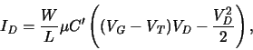
$\displaystyle Q'(x)$ $\textstyle =$ $\displaystyle C'\left(\ensuremath{V_{\mathit{G}}}\xspace -\ensuremath{V_{\mathit{T}}}\xspace -\Psi(x)\right),$ (A.1)
$\displaystyle E_x(x)$ $\textstyle =$ $\displaystyle -\frac{d\Psi(x)}{d x},$ (A.2)

where $C' = \ensuremath{\epsilon _{\mathit{i}}}\xspace /\ensuremath{t_{\mathit{ins}}}\xspace $ is the capacitance per area. The current can then be written as

\begin{displaymath}
\ensuremath{I_{\mathit{D}}}\xspace = W Q'(x) \mu E_x(x) =
...
...ath{V_{\mathit{T}}}\xspace -\Psi(x)\right)\frac{d\Psi(x)}{dx}
,\end{displaymath} (A.3)

where $\mu$ is the charge carrier mobility. Integrating (A.3) from x=0 to L finally gives

\begin{displaymath}
\ensuremath{I_{\mathit{D}}}\xspace = \frac{W}{L} \mu C' \le...
...ace - \frac{\ensuremath{V_{\mathit{D}}}\xspace ^2}{2} \right)
,\end{displaymath} (A.4)

which holds for $\ensuremath{V_{\mathit{D}}}\xspace < \ensuremath{V_{\mathit{G}}}\xspace -\ensuremath{V_{\mathit{T}}}\xspace $. As the current varies linarly with the control voltage \ensuremath{V_{\mathit{G}}} this is also called the linear region of operation. As the channel potential rises towards the drain the charge density decreases, i.e., the channel gets thinner at the drain side. When $\ensuremath{V_{\mathit{D}}}\xspace > \ensuremath{V_{\mathit{G}}}\xspace -\ensuremath{V_{\mathit{T}}}\xspace $ the charge density Q'(x) would approach zero before the drain at some x = L' < L which is called the pinch-off point, requiring an infinite lateral field to maintain the current. However, the model loses its validity before this point as the lateral field was assumed to be small compared to the vertical one. Further analysis of Poisson's equation without the gradual-channel approximation, i.e., including a term $\ensuremath{\epsilon _{\mathit{s}}}\xspace \partial^2\Psi/\partial x^2$ in the charge density does not lead to an analytical current expression, but it shows that both Ex and Q' remain finite and the current saturates at about

\begin{displaymath}
\ensuremath{I_{\mathit{D}}}\xspace = \frac{W}{L} \frac{\mu ...
..._{\mathit{G}}}\xspace -\ensuremath{V_{\mathit{T}}}\xspace )^2
.\end{displaymath} (A.5)

The channel length modulation L'/L is neglected. Therefore, this operating region is also called the saturation region.

(A.4) and (A.5) are most widely used throughout literature. Yet, whenever using these equations it should be kept in mind that they were derived from the rather simple structure in Fig. A.1, which may not reflect the physical behavior of the considered devices.


next up previous contents
Next: A.1.2 The Concrete MOSFET Up: A.1 MOS Transistors Previous: A.1 MOS Transistors

G. Schrom