


Next: A.1.2.1 Strong Inversion
Up: A.1 MOS Transistors
Previous: A.1.1 The Field Effect
A.1.2 The Concrete MOSFET (I): Long-Channel Transistors
A modified version of the rather hypothetical device in
Fig. A.1 is shown in Fig. A.2.
A legend of materials is shown Fig. A.19).
It consists of a
metal-oxide-semiconductor (MOS) structure, where the metal (or doped
polysilicon) forms the gate, the oxide acts as gate insulator, and
the semiconductor makes up the area of the channel and below.
The four terminals S, G, D, and B are
referred to as source, gate, drain, and bulk, respectively.
The n+ doped regions contact the channel which
forms below the semiconductor-oxide interface.
The basic operation principle is the same as for the device
in Section A.1.1: the electric field at the oxide-semiconductor
interface controls the electron density in the semiconductor.
The p doped region below the channel is depleted to a
certain depth
 |
(A.6) |
with
 ,
so that the negative acceptor charges,
together with the gate oxide thickness and the work function differences
of the gate and contact materials determine the threshold voltage
(for a detailed derivation see [2,81]):
,
so that the negative acceptor charges,
together with the gate oxide thickness and the work function differences
of the gate and contact materials determine the threshold voltage
(for a detailed derivation see [2,81]):
 |
(A.7) |
For n-type polysilicon as gate material the workfunction
difference evaluates to
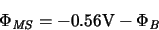 |
(A.8) |
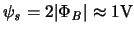
with the built-in potential defined as
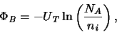 |
(A.9) |
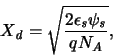
and the body factor
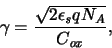 |
(A.10) |
where
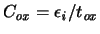 is the gate capacitance per area and
 is the acceptor concentration.
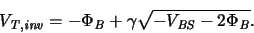
In the presence of fixed charges at the interface the threshold voltage
shifts by
is the acceptor concentration.
In the presence of fixed charges at the interface the threshold voltage
shifts by
 .
.
Figure A.2:
Principle structure of a MOSFET
![\includegraphics[scale=1.0]{long-fet.eps}](img703.gif)
|
Next: A.1.2.1 Strong Inversion
Up: A.1 MOS Transistors
Previous: A.1.1 The Field Effect
G. Schrom