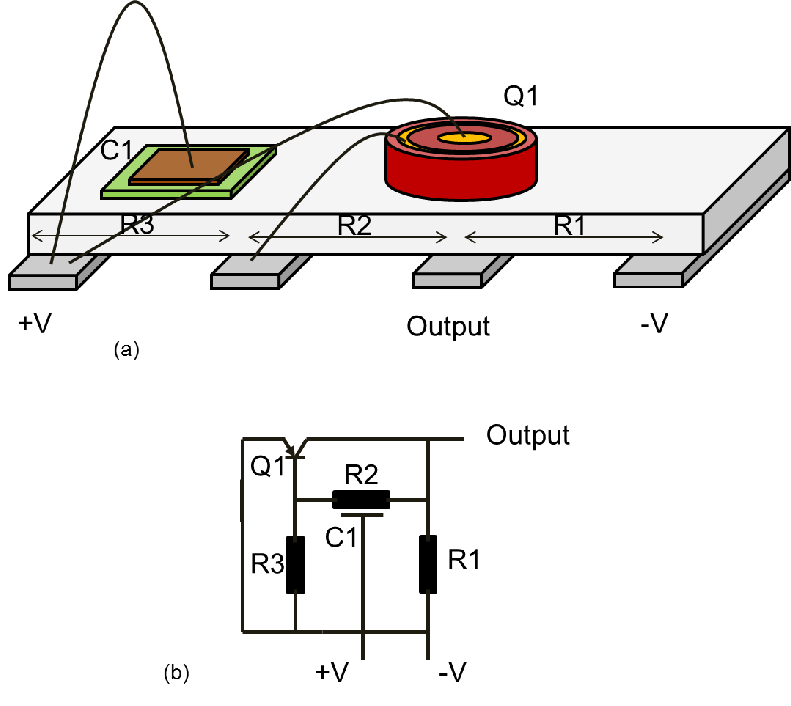
| Figure 1.1.: | Kilby’s device with mesa components (a) and circuit description of the single-transistor oscillator (b). Image based on [8]. |
By the end of World War II, the power of computational devices was brought to the society attention and, by the advent of mechanical and electrical machines, their advancement has reached the technological limits of the time. These machines were responsible for the automation of complex calculation procedures, such as projectile trajectories and cryptography. A famous example is the crack of the cryptography messages produced by the German machines known as Enigma [1]. At the time, the British army built a decrypt machine named Bombe based on an earlier Polish technology. The Bombe was 2.1m wide, 1.98m tall and 0.61m deep and weighted approximately one ton [1]. It was an enormous machine which was dedicated to perform an algorithm which fits today in a few hundreds lines of code and which can be executed in almost every modern computer. The technological revolution which allowed this miniaturization outbreak began in the mid of 1950s with the first steps towards the invention and realization of the integrated circuit (IC).
Contrary to common sense, IC invention was not driven mainly by miniaturization of electronic devices, but by the need for reliability [2][3]. The first general purpose computer known as ENIAC had 17468 vacuum tubes, 7200 crystal diodes, 1500 relays, 70000 resistors, 10000 capacitors and around 5 million hand-soldered joints [4]. Having a vacuum tube burn out was quite a common occurrence during the warm-up or cool-down process, and every failure had to be manually fixed. There are rumors which state that ENIAC has had a non-operation time of 50%, which is quite unlikely. At the height of ENIAC reliability technology the computer was able to operate, on average, every 2 days without burning a tube [5]. The invention of the transistor in 1947 eliminated the problems associated with the vacuum tubes as electronic devices became more reliable [6]. However, the need for more computation power required more devices. The huge amount of electronic devices led to the problem known as “Tyranny of numbers” [6]. The design of new devices was very complex and the amount of wiring connections required between the components was absurd, considering they all needed to be done manually. A solder fail was quite a frequent event which was very difficult to locate and to diagnose.
Circuit integration was presented as a solution for this reliability problem [2][3][6]. The idea of manufacturing electronic components in a monolithic piece of semiconductor was very tempting. The number of manually wired connections would be drastically reduced and more than one device could be manufactured at once, reducing the production costs. However, circuit integration faced three major challenges at the beginning of the 1950s [7]. First, for the integration itself, there was no available technology which was able to create different components on a single semiconductor substrate. Second, the isolation: if a multiple number of components were successfully produced in a single substrate, they would need to be electrically isolated from each other. However, nobody really knew how to do this, at the time. Lastly, the interconnections: there was no financially feasible solution to electrically connect the integrated components.
The first successful solution for integration was developed by Jack Kilby in the summer of 1958 [8][9]. He realized that all circuit elements (e.g. resistors and capacitors) could be made using a semiconductor material, moreover they can be formed on a single substrate. Kilby used several earlier developments such as mesa transistor and mesa diodes to build a single-transistor oscillator with a distributed RC feedback. It is considered by many the first IC ever made, a schematic of which is shown in Fig. 1.1 [2][3].
| Figure 1.1.: | Kilby’s device with mesa components (a) and circuit description of the single-transistor oscillator (b). Image based on [8]. |
Kilby’s biggest contribution was to show that any electrical component could be built in a single chip. However, his implementation had some flaws; the device isolation was made by cutting grooves and the connections were manually wired.
At the end of 1958, Kurt Lehovec developed a method to electrically isolate multiple components which are placed on a single substrate[10]. He claimed that the use of several p-n junctions in series could prevent current flow between the elements. The junction could be biased, if needed, in the blocking direction. Lehovec’s idea was successfully tested using the structure depicted in Fig. 1.2.
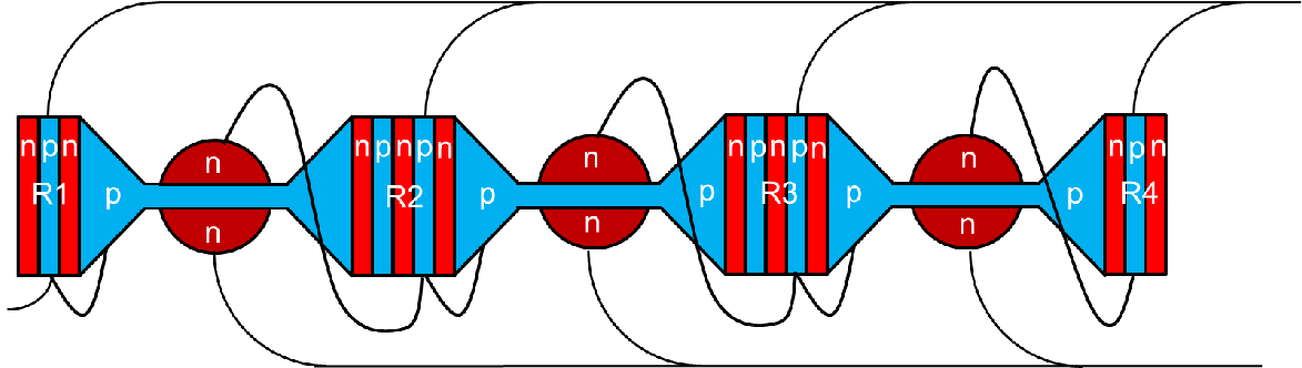
| Figure 1.2.: | Schematic of the device constructed by Lehovec. The PN junction in series works as a barrier to prevent the undesired current flow through the silicon. Image based on [10]. |
In 1959 Robet Noyce developed, based on Jean Hoerni’s work, the manufacturing process, which would enable the adaptation of ICs on large scale. He adapted the ideas of Kilby and Lehovec to the new planar transistor developed by Hoerni [11]. The process of planar transistor fabrication is very similar to the manner in which devices are fabricated today. The process is initiated with an undoped silicon wafer covered by a layer of silicon oxide. Then, a window is opened by photolithography in the corresponding device planned location. Finally, impurities are diffused to form the conduction wells and the planar transistor is complete. A summary of the process is depicted in Fig. 1.3.
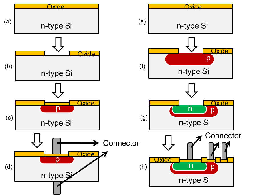
| Figure 1.3.: | Description of the planar process developed by Jean Hoerni for a diode (left side) and a transistor (right side). A sample of an n-type Silicon substrate is prepared with silicon oxide on top (a and e). In predetermined regions the oxide is etched (b and f), opening spots for impurity diffusion (c, f, and g). After diffusion, an oxide layer is regrown in the etched openings and the metal contacts are deposited (d and h). Image based on [11]. |
In addition to the planar process, Noyce developed a method to make the electrical connections of the devices without manual intervention. The idea was quite obvious after the development of the planar transistor; it consists of the preservation of the oxide layer on the top of the device (except on the contact points with the active regions). In that way, metal layers could be deposited on the oxide, which would work as isolation between the metal interconnections and the substrate.
The invention of ICs was the object of discussion for several years, which led to a patent war between several leading electrical companies [2]. For many years the invention was mainly accredited to Jack Kilby and Robert Noyce. But in 2000, only Jack Kilby received the physics Nobel prize “for his part in the invention of the integrated circuit” [12]. This led to a new debate of the legitimate inventors of the IC, but in the end the invention of the IC is viewed as a collaborative result with contributions from several engineers and scientists, which improved the fabrication process step by step until enabling mass production.