| Figure 1.8.: | A conceptual example of 2.5D technology. The silicon interposer is used to reduce the connection paths between the chips. |
There are many expectations surrounding 3D integration [31]. Some commercial applications are already available on the market, but there is a general feeling in the engineering community that a “killer application” is missing. Actually, the mass production of 3D devices in the mainstream is not yet a reality. The technology still faces many challenges [33]. In the processing steps, TSVs suffer from high mechanical and thermal stresses, which compromises their structural stability. Obtaining a high yield is also a concern, since an economically viable yield rate is difficult to achieve. There are also open concerns during device operation, such as thermal management being of particular concern. The piling up of devices can hinder the thermal dissipation and temperatures beyond the devices’ operation range can be easily reached. In addition to the process and operation issues there is also a lack of software design tools. A 3D IC needs a specific tool for design and the currently available software is unable to handle the particularities of this technology. Finally, the last obstacle involves test. New methodologies to probe the devices are needed, especially the devices which are found in the lower layers.
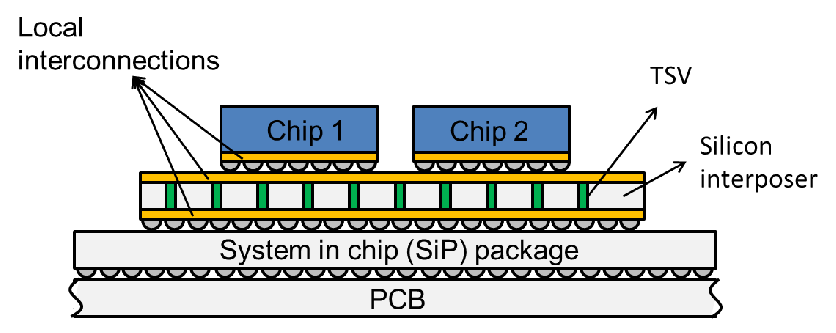
Judging by the amount of obstacles, it appears unlikely that the realization of 3D IC technology is feasible in the near future in a large volume. However, such analysis shows a very pessimistic view. The 3D IC technology based on TSVs is already available on some markets for commercial applications, especially sensors and digital cameras [34][35]. Naturally, very high density integration is not the goal of these markets but they point in the direction which could lead to solving the problems associated with this technology. TSVs are also being employed in so called 2.5D technologies such as interposers [36]. The dies are not piled up but instead, they can be placed closer to each other, thereby reducing metal lines length as depict in Fig. 1.8.
| Figure 1.8.: | A conceptual example of 2.5D technology. The silicon interposer is used to reduce the connection paths between the chips. |