Next: 3. Defect Creation Up: 2. Carrier Transport Previous: 2.5 The Spherical Harmonics Expansion
As described above, theoretical models and simulation approaches have been continuously improved and implemented in simulators by various scientific groups. The improvements and developments of some groups already spans decades and continues at the present moment. A list of used simulation tools employed in this work is presented below.
The employed simulation procedure to calculate the carrier DF consists of several steps, and is described by the flowchart shown in Figure 2.5.
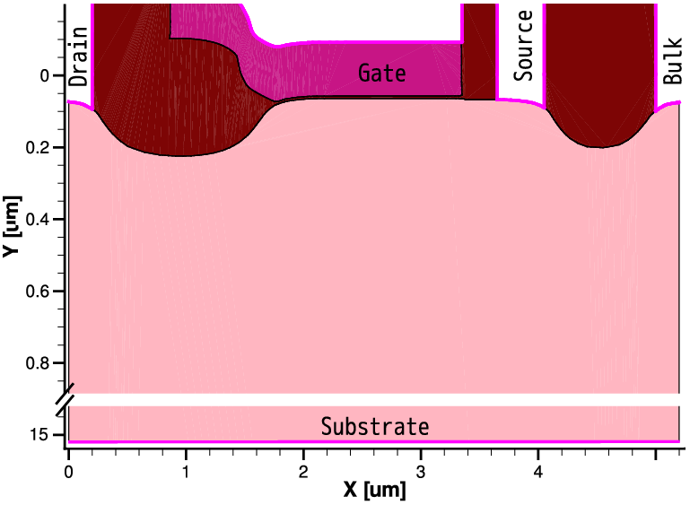
The device topology with a doping profile is obtained from the process simulator and is used as input data for the initial MiniMOS-NT simulation. During this simulation, potential and carrier density distributions are calculated for the chosen stress voltages. The resulting information is then used as input data for MONJU with a NSC/MR approach and for the optimization of the device topology. In some cases, the silicon bulk of the transistor may be as large as 15um. It is obvious that the calculation of the physical quantities using the MC approach is a challenge for such a huge area. Moreover, according to the suggested scheme for HCD modeling, one is interested only in the carrier distribution function at the device interface. Therefore, the simulation efficiency can be increased by reducing the size of the silicon bulk, e.g. the device can be cut at the potential profile saturation point. Furthermore, in the present MC device simulators [154,157], because of computational efficiency, a rectangular grid is used. That is, due to the different types of the simulation grid which are used by MiniMOS-NT and MONJU (triangular and rectangular, respectively), data conversion is necessary. It should be mentioned that the realization of the MC method is possible in the case of triangular grid type but leads to a significant increase of the computational time. An example of the converted n-type LDMOS transistor is demonstrated in Figure 2.6. At the final step of the transport block, the carrier DF is calculated by MONJU. Note, there is no requirement to perform the full procedure every time from the beginning. Several steps, such as the device geometry optimization might be omitted in the case of subsequent simulations.
 (b)
(b)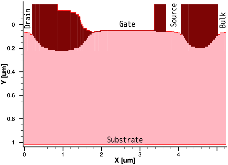
|
