Next: 3.4 Impact of the Carrier Distribution Function on HCD Modeling Up: 3. Analysis of Worst-Case HCD Conditions in the Case of n- and p-channel MOSFETs Previous: 3.3.1 WCC of Long-Channel Devices
The developed approach for WCC analysis is applicable in the case of HV LDMOS transistors. A cross section of devices employed for the analysis of the model applicability for such a type of devices is shown in Figure 3.12. The first HV transistor is an n-type LDMOS integrated into an 180nm CMOS base process (Figure 3.12a). A 350nm thick shallow trench isolation (STI) oxide is used as a dielectric layer above the drift region of the high voltage device. The second device is a HV p-type LDMOS with a simplified geometry (flattened interface and absence of the STI, see Figure 3.12b). The operation voltage of these transistors is Vgs = 20V and Vds = -20V, respectively. Following the same computational procedure as described above, the maximum value of the acceleration integral as a function of {Vds,Vgs} is calculated. The graphs obtained confirm the tendency that for the case of a n-type LDMOS the WCC are realized at the maximum Isub. In contrast, for the p-type LDMOS, the severest HCD corresponds to the maximum gate current. This detailed picture agrees with the empirical concept concerning the HCD worst-case conditions documented in literature.
(a)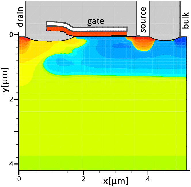 (b)
(b)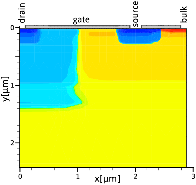
(c) 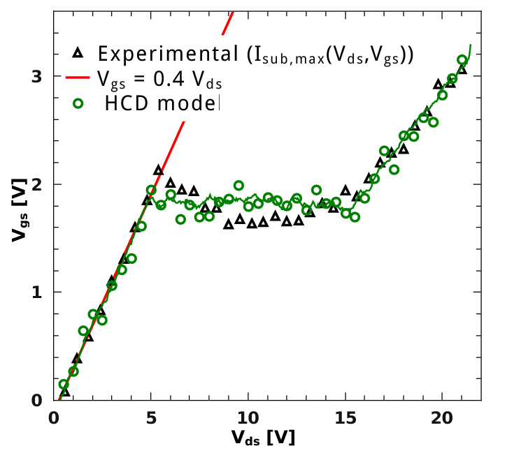 (d)
(d)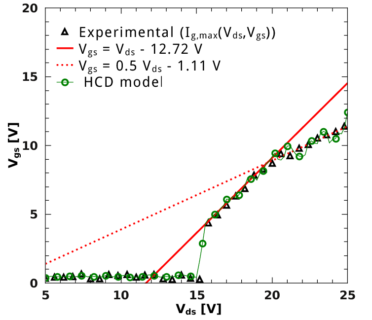
|
Finally, it is possible to conclude that the developed HCD model reproduces the WCC with a reasonable accuracy. The simulated diagrams representing the maximum AI as a function of gate and drain voltages agree well with the color maps Isub = Isub(Vds,Vgs) for n-MOSFETs and Ig = Ig(Vds,Vgs) for p-MOSFETs. Moreover, the suggested approach for HCD modeling predicts the position where the most degraded device section is localized (i.e. between the drain end of the gate and the drain in the case of long-channel devices).