Next: 3.3.2 WCC of High-Voltage Up: 3. Analysis of Worst-Case HCD Conditions in the Case of n- and p-channel MOSFETs Previous: 3. Analysis of Worst-Case HCD Conditions in the Case of n- and p-channel MOSFETs
 (b)
(b)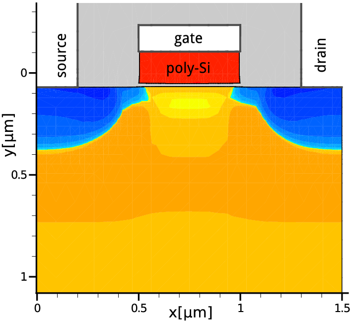
|
The WCC of hot-carrier degradation in the case of a long-channel n-MOSFET are reached when the substrate current Isub is at its maximum [70,167,29,41]. It is usually assumed that this maximum corresponds to Vgs≅ (0.4-0.5)Vds. As for long-channel p-MOSFET, WCC are observed at the maximum gate current Ig and an empirical link between the voltages is not established [50,51,52].
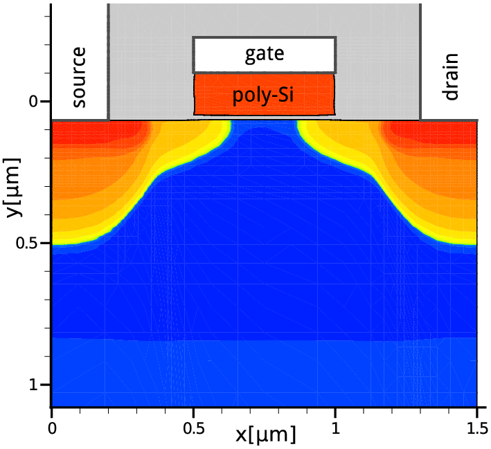
Long-channel n- and p-MOSFETs with a metallurgical gate contact length of 0.5um (the device architectures and the net doping profiles are sketched in Figure 3.9) have been employed for monitoring the criteria reflecting the severity of HCD. All lateral coordinates x refer to an origin placed at the left edge of the source contact for both devices. Together with a relatively high operation voltage this channel length ensures that the single-electron mechanism of the Si-H bond dissociation is the dominating one [41]. In the case of n-MOSFETs, the substrate current as a function of varying {Vds,Vgs} was recorded and binned onto a color map (Figure 3.10a). For p-MOSFET Ig = Ig (Vds,Vgs) was measured and depicted in Figure 3.10b.
(a)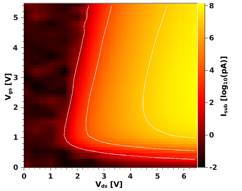 (b)
(b)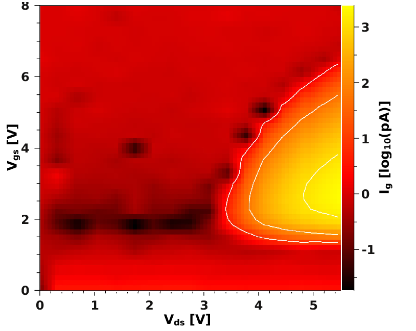
(c) 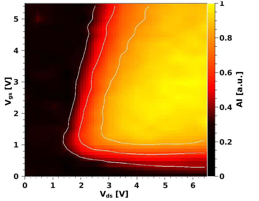 (d)
(d)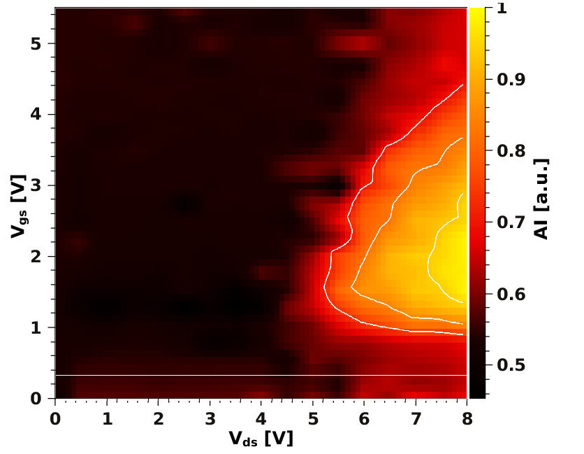
|
Note that in a previous Section 3.2 the damage produced by channel holes is also considered. However, in Section 3.1 it is shown that in the case of the channel length of 0.5um the linear drain current degradation is sufficiently described by the electron contribution only. Furthermore, as discussed in Section 3.1 the dose of damage provided by the MP-component is homogeneously distributed over the lateral coordinate. This is because the prefactor in the MP-induced interface state concentration defined by the acceleration integral is already saturated due to the high concentration of relatively "cold" carriers (represented by the low-energy fragment of the DF). As a result, the non-uniform nature of HCD is related to the single-carrier bond-breakage process with the corresponding contribution to the total interface state density localized near the drain end of the gate. Therefore, in order to find the stress conditions corresponding to the worst-case scenario, it is suggested to analyze the behavior of the acceleration integral, without considering the interaction between the SP- and MP-mechanisms. In literature, one may find other criteria how efficiently carriers interact with the bond, i.e. the maximum of the electric field, the carrier dynamic temperature, position where the DF demonstrates most extended high-energy tales, etc. However, as it will be additionally confirmed in the next chap:cptech, the Nit peak only corresponds to the maximum of the AI and is shifted with respect to maxima of other quantities.
(a)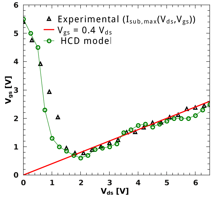 (b)
(b)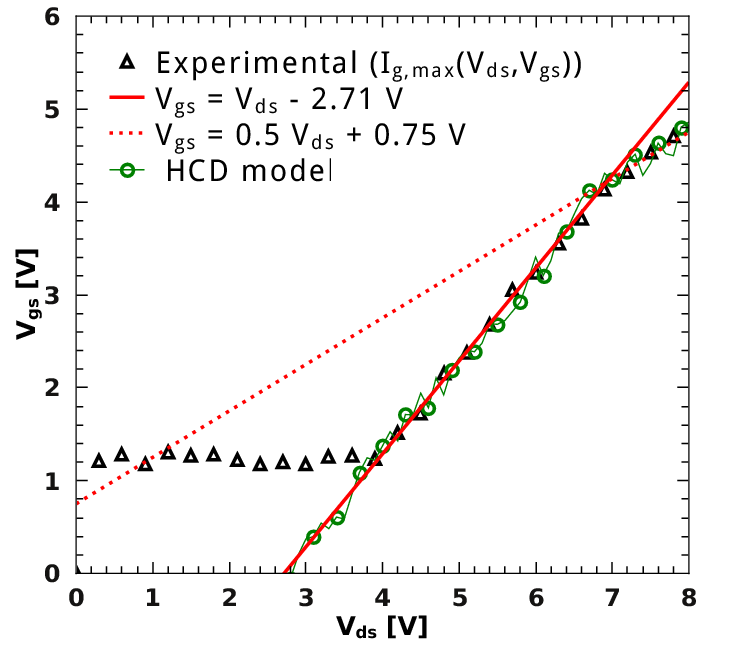
(c) 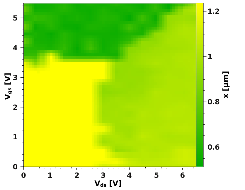 (d)
(d)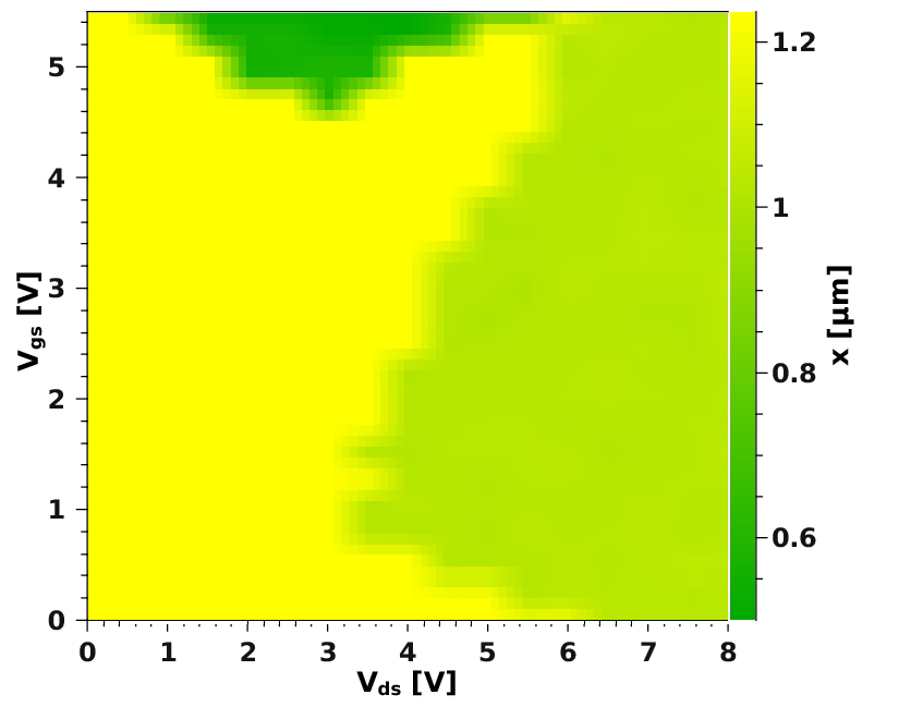
|
In order to numerically calculate picture for the worst-case conditions, the following computational procedure is used. The carrier acceleration integral is used as a criterion to judge how severe the HCD is. In other words, the AI as a function of {Vds,Vgs} is calculated and the color maps (see Figure 3.10c and Figure 3.10d) is produced in the same fashion as Figure 3.10a and Figure 3.10b, respectively. The computational procedure presumes the following steps. Initially, Vgs and Vds are varied in the range of 0..6V and 0..7V (for p-MOSFET the Vds range is of 0..8V) with 0.2V step. For each pair {Vds,Vgs} the set of carrier DFs (i.e. at each point along the Si/SiO2 interface) is calculated. This information is used to calculate the dependences of the carrier acceleration integral vs. the lateral coordinate. After processing these dependencies the maximum value of the acceleration integral ISP is plotted as a function of {Vds,Vgs}. Therefore, the entire computational routine contains approximately 1000 different combinations of stress voltages while each pair {Vds,Vgs} includes time expensive Monte-Carlo simulations of the carrier DF.
The comparison between Figure 3.10a (Figure 3.10b) and Figure 3.10c (Figure 3.10d) demonstrates a good agreement between experimental and simulated color maps for both types of transistors. The dependence of the gate voltage on the drain bias corresponding to the worst-case conditions is also plotted, see Figure 3.11a and Figure 3.11b. This data is extracted from igure 3.10a and Figure 3.10b where Vgs is presented as a function of Vds which is found as the value guaranteeing the maximum of either experimental data (Isub for n-MOSFET and Ig for p-MOSFET) or ISP (simulations with HCD model) for a chosen value of Vds. For a drain voltage above ~2.0V for the n-MOSFET this dependence follows the law Vgs = 0.4 Vds typical for this device. Although for the p-MOSFET this dependence is more complicated (Figure 3.11b), the experimental and simulated pictures are in good agreement. Finally, the position where the maximum AI is observed is plotted vs. {Vds,Vgs}, see Figure 3.11c and Figure 3.11d. Since the peak of the acceleration integral determines the location of the most severe degradation spot, this graph can be used to predict where the most degraded section of the device is located. Note that the color maps presented in Figure 3.11c and Figure 3.11d reflect the pattern shown in Figure 3.10c and Figure 3.10d, respectively. For instance, the orange area pronounced in Figure 3.10d (and bordered by the right contour curve) corresponds to the light green spot in Figure 3.11c.