Next: 4.1.2 Effective Channel Length Up: 4.1 Basic Principles of Charge Pumping Measurements Previous: 4.1 Basic Principles of Charge Pumping Measurements
(a)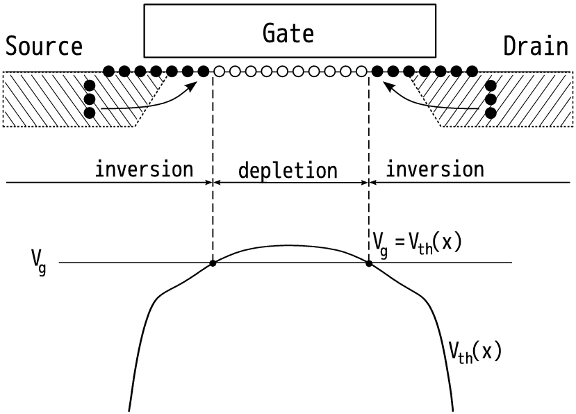 (b)
(b)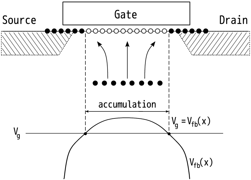
|
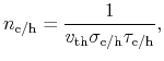
Foremost, it is necessary to introduce the notion of local threshold and local flatband voltages [173]. These quantities describe the dependencies of CP characteristics on the gate pulse amplitude VA, the frequency f, the reverse bias on source and drain, etc. Moreover, the mentioned values are the key parameters for the determination of lateral defect distributions. The local threshold voltage Vth(x) can be defined as the gate voltage required to induce a certain density of minority carriers (electrons in the case of n-type MOSFET) and the local flatband voltage Vfb(x) is the gate voltage required to induce a desired density of majority carriers (holes) at each position x along the Si/SiO2 interface. The values of these densities should be defined such that the interface states can capture holes and electrons during the inversion and accumulation periods of the gate pulse [173]. In other words, Vth(x) and Vfb(x) depend on the dynamics of the capture and emission process at the interface. The distribution of Vth(x) and Vfb(x) can be calculated with the device simulator MiniMOS-NT using a widely-adopted routine [173,174,22,175,176]. Namely, as it was explaned above, the local threshold (flatband) voltage of a point at the interface of an n-type MOSFET is defined as the gate voltage required to accumulate the electron (hole) concentration ne/h [173]
wherevth | - thermal carrier velocity ( = 1× 107cm/s), |
τe/h | - time constant for electron (hole) trapping ( = 1/(2f)), |
σe/h | - capture cross section for electrons (holes). |
Consequently, the dependence of the local threshold and flatband voltages on the coordinate along the interface x is determined by the oxide thickness and the amount of charges in the oxide and/or at the device interface. Additionally, these voltages significantly change with the position around the drain/source junctions as a result of variations in impurity concentration and two-dimensional effects in the potential. As shown in Figure 4.2a, an interface of an n-type MOSFET with a local threshold lower than Vg is flooded with electrons supplied from the source or drain. Similarly, as shown in Figure 4.2b, an interface whose local flatband voltage is higher than Vg is filled with holes from the substrate. Furthermore, it is necessary to consider the dynamic response of free carriers around the drain contact when periodic pulses of high level Vgh and low level Vgl are applied to the gate electrode. When Vg equals Vgh, the interface between the drain and x1 is flooded with electrons from the drain (see, Figure 4.3). Simultaneously, the holes are rapidly swept into the substrate. As a consequence, interface states in this region are emptied of holes. However, when Vg falls to Vgl, free electrons go back to the drain and holes flood back from the substrate again and reach x2. This tendency is reflected in Figure 4.3. Therefore, the interface traps up to x2 are filled with holes.
|