As already discussed in previous sections the influence of the drain potential on the channel region can have serious impact on the performance of sub-micron MOS transistors. One effect that is very similar to the punchthrough effect is Drain-Induced Barrier Lowering (DIBL) [74]. In the literature punchthrough is sometimes referred to as ``subsurface DIBL'' in contrast to ``surface DIBL'' which will be described in this section.
In the weak inversion regime there is a potential barrier between the source and the channel region. The height of this barrier is a result of the balance between drift and diffusion current between these two regions. If a high drain voltage is applied, the barrier height can decrease, as indicated in Fig. 2.6, leading to an increased drain current. Thus the drain current is controlled not only by the gate voltage, but also by the drain voltage. For device modeling purposes this parasitic effect can be accounted for by a threshold voltage reduction depending on the drain voltage [13].
![\resizebox{0.95\textwidth }{!}{
\psfrag{xlabel} [ct][ct] {lateral position $x$\ ...
...5}
\includegraphics[width=0.95\textwidth ]{../figures/phenomena-surfacepot.eps}}](img53.gif)
|
The DIBL effect becomes obvious when looking at the transfer curves of a MOS
transistor for the linear and saturated cases (Fig. 2.7). If there was no
DIBL, the two curves would coincide in the subthreshold regime. The DIBL
effect can be measured by the lateral shift of the transfer curves in the
subthreshold regime
![]() divided by the drain voltage difference of
the two curves and is given in units (mV/V):
divided by the drain voltage difference of
the two curves and is given in units (mV/V):
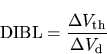 |
(2.9) |
![\resizebox{0.95\textwidth }{!}{
\psfrag{xlabel} [ct][ct] {gate voltage {
{$V_{\m...
...c] {1.5}
\includegraphics[width=0.95\textwidth ]{../figures/phenomena-dibl.eps}}](img56.gif)
|