In order to evaluate the average gate delay time of an infinite inverter
chain, an adequate model for one single stage has to be created
(Fig. 6.2). It consists of a CMOS inverter built up by NMOS and
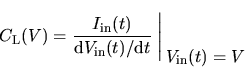
PMOS transistors and a capacitive load ![]() connected to the output
of the inverter stage. This capacitor accounts for the gate capacitance of the
following stage and, since it changes during transition, it is assumed to be
voltage dependent. It can be calculated using the input current information of
the succeeding stage supposing that the input voltage
connected to the output
of the inverter stage. This capacitor accounts for the gate capacitance of the
following stage and, since it changes during transition, it is assumed to be
voltage dependent. It can be calculated using the input current information of
the succeeding stage supposing that the input voltage ![]() is a
monotonous function of time (which will be discussed in
Section 6.2.2):
is a
monotonous function of time (which will be discussed in
Section 6.2.2):
The interconnect capacitances are neglected here, therefore this model represents the ideal case and the resulting delay time will be a lower limit set by the intrinsic quantities of the devices only.
The model is evaluated for the two switching cases, the on- and off-transitions of the output node. Therefore, there exist two different C-V curves, each corresponding to one possible transition.
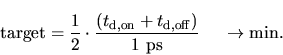
The optimization target which will be minimized during optimization, is
defined as the average inverter delay time for the on- and off-transitions:
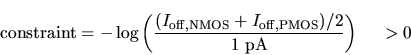
The optimization constraint which is kept above zero, guarantees that the
average leakage current stays below 1pA. In contrast to the constraint
definition for the drive current optimizations (4.2) the average
leakage currents of the NMOS and PMOS transistors have to be taken into
account here, assuming that the likelihoods that the inverter is in the on- or
off-state are the same, which is true for an inverter chain:
![\resizebox{0.5\textwidth}{!}{
\psfrag{NMOST} [rc][rc] {NMOS}
\psfrag{PMOST} [rc]...
...}
\includegraphics[width=0.5\textwidth]{../figures/inverterstage-gatedelay.eps}}](img184.gif)