The major objective of small-signal simulations is to extract various figures of merit of the devices or networks. Two-port parameter sets are useful design aids provided by manufactures for high-frequency transistors. In addition, they are used to extract the cut-off frequency or the maximum oscillation frequency, which are further required for characterization of the devices. The following basic definitions are generally used [164]:
| Impedance |
|
|
| Resistance |
|
 |
| Reactance |
|
 |
| Admittance |
 , , |
|
| Conductance |
|
 |
| Susceptance |
|
 |
Furthermore, a distinction between intrinsic and extrinsic parameters has to be made. Measured admittance and scattering parameters are normally different from the simulation results. If the errors are systematically introduced by the measurement environment, it is useful to represent the device as embedded in a parasitic equivalent circuit. Hence, the intrinsic parameters represent the de-embedded device. Based on a standard parasitic equivalent circuit, the simulator can take all parasitics into account and can calculate also extrinsic two-port parameters.
In order to clarify the notation of the various parameters hereafter, the
following definition shall be used:
![]() refers to a specific
complex-valued admittance value, however for the sake of readability Y as in
Y-parameters refers to a general admittance quantity. A lower case letter for
an intrinsic parameter is sometimes used to distinguish from extrinsic
parameters written with an upper case letter. For the sake of clarification,
this distinction is not made in this work and the context of the respective
parameter is always clearly indicated.
refers to a specific
complex-valued admittance value, however for the sake of readability Y as in
Y-parameters refers to a general admittance quantity. A lower case letter for
an intrinsic parameter is sometimes used to distinguish from extrinsic
parameters written with an upper case letter. For the sake of clarification,
this distinction is not made in this work and the context of the respective
parameter is always clearly indicated.
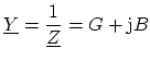
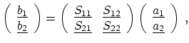
An ![]() -port device/network can be represented by several matrices or parameter
sets. At low frequencies, these are usually Y-, Z-, H-, or A-matrices or parameters,
because they can be easily measured with open or short circuits.
-port device/network can be represented by several matrices or parameter
sets. At low frequencies, these are usually Y-, Z-, H-, or A-matrices or parameters,
because they can be easily measured with open or short circuits.
For a two-port device/network as depicted in Figure 3.1, they are defined as follows:
 |
(3.1) |
 |
(3.2) |
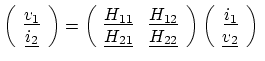 |
(3.3) |
 |
(3.4) |
Hybrid (H-) parameters are often used for the description of active
devices such as transistors. Like Y-parameters, they are difficult to measure
at high frequencies. The absolute value of the
![]() parameter is used
to characterize
parameter is used
to characterize
![]() , where the current gain has dropped to unity. The
so-called chain or A-parameters, sometimes also referred to as ABCD-parameters,
are useful for cascaded circuit topologies, since these parameters allow matrix
multiplications of the single elements:
, where the current gain has dropped to unity. The
so-called chain or A-parameters, sometimes also referred to as ABCD-parameters,
are useful for cascaded circuit topologies, since these parameters allow matrix
multiplications of the single elements:
 |
(3.5) |
Advanced devices are operated under their originally intended environment
conditions for higher frequencies above ![]() MHz. A steady-state bias is
applied to all terminals superimposed by an additional RF excitation. The
sinusoidal currents and voltages of all terminals with magnitude and phase
should be measured. This would normally involve Z-, Y-, H- and A-parameters of
the linear two-port theory, which are able to completely describe the
electrical properties of the device. Unfortunately, three main problems can be
identified [45]:
MHz. A steady-state bias is
applied to all terminals superimposed by an additional RF excitation. The
sinusoidal currents and voltages of all terminals with magnitude and phase
should be measured. This would normally involve Z-, Y-, H- and A-parameters of
the linear two-port theory, which are able to completely describe the
electrical properties of the device. Unfortunately, three main problems can be
identified [45]:
To avoid these drawbacks, S-parameters can be used to characterize a two-port
network, which are related to the scattering and reflection of traveling waves
(power or equivalent voltage waves). Instead of open and short termination, the
ports are terminated by a cable of the characteristic impedance ![]() . The
device is so embedded into a transmission line of a certain characteristic
impedance
. The
device is so embedded into a transmission line of a certain characteristic
impedance ![]() , usually 50
, usually 50![]() . This scattering and reflection is
comparable to optical lenses which transmit and reflect a certain amount of
light. The traveling waves can so be interpreted in terms of normalized voltage
and current amplitudes. S-parameters are the complex-valued reflection
coefficients at each port and complex-valued transmission coefficients of the
equivalent voltage wave between each pair of ports. Hence, an
. This scattering and reflection is
comparable to optical lenses which transmit and reflect a certain amount of
light. The traveling waves can so be interpreted in terms of normalized voltage
and current amplitudes. S-parameters are the complex-valued reflection
coefficients at each port and complex-valued transmission coefficients of the
equivalent voltage wave between each pair of ports. Hence, an ![]() -port
device or circuit with
-port
device or circuit with ![]() S-parameters has
S-parameters has ![]() reflection coefficients and
reflection coefficients and ![]() transmission coefficients. An additional advantage is the fact, that
traveling waves do not vary in magnitude at points along a lossless
transmission line. In contrast to other parameter measurements, S-parameters
can be measured at some distance from the measurement transducers
[98].
transmission coefficients. An additional advantage is the fact, that
traveling waves do not vary in magnitude at points along a lossless
transmission line. In contrast to other parameter measurements, S-parameters
can be measured at some distance from the measurement transducers
[98].
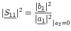
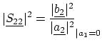
S-parameters provide detailed information on the linear behavior of the two-port. As shown in Figure 3.2, they are basically defined as follows:
 |
(3.6) |
|
(3.7) |
|
|
|
|
|
|
 |
|
 |
|
 |
|
 |
|
The parameters
![]() and
and
![]() are obtained by terminating the
port 2 by a perfect
are obtained by terminating the
port 2 by a perfect ![]() load (
load (
![]() ) and measuring the incident,
reflected, and transmitted signals. Parameter
) and measuring the incident,
reflected, and transmitted signals. Parameter
![]() is equivalent to the
complex-valued input reflection coefficient (impedance) of the device and
is equivalent to the
complex-valued input reflection coefficient (impedance) of the device and
![]() is the complex-valued forward transmission coefficient. In turn,
while terminating port 1 by a perfect load (
is the complex-valued forward transmission coefficient. In turn,
while terminating port 1 by a perfect load (
![]() ), the parameters
), the parameters
![]() and
and
![]() are measured, which are the complex-valued output
reflection coefficient (output impedance) or reverse transmission coefficient,
respectively. The accuracy of the measurements strongly depends on the quality
of the terminations. If the perfect load cannot be established, the S-parameter
definition requirements are not met.
are measured, which are the complex-valued output
reflection coefficient (output impedance) or reverse transmission coefficient,
respectively. The accuracy of the measurements strongly depends on the quality
of the terminations. If the perfect load cannot be established, the S-parameter
definition requirements are not met.
The magnitudes of the reflection parameters
![]() and
and
![]() ,
which are always smaller than 1, can be interpreted as follows: In the case
of -1, all voltages are inverted and reflected (0
,
which are always smaller than 1, can be interpreted as follows: In the case
of -1, all voltages are inverted and reflected (0![]() ), zero means
perfect impedance matching and no reflections (50
), zero means
perfect impedance matching and no reflections (50![]() ), and at +1 all
voltages are reflected (
), and at +1 all
voltages are reflected (
![]() ).
).
In the case of an active amplification, the magnitudes of the transfer
parameter
![]() and reverse parameter
and reverse parameter
![]() can be larger than
can be larger than
![]() . They can also start at a negative value in the case of a phase
inversion. If the magnitude is zero, there is no signal transmission, between
0 and
. They can also start at a negative value in the case of a phase
inversion. If the magnitude is zero, there is no signal transmission, between
0 and ![]() a damping takes place, at
a damping takes place, at ![]() there is a unity gain transmission
and above
there is a unity gain transmission
and above ![]() an input signal amplification.
an input signal amplification.
![]() on the real-valued axis characterize Ohmic resistors.
on the real-valued axis characterize Ohmic resistors.
![]() above the real-valued axis characterize inductive impedances.
above the real-valued axis characterize inductive impedances.
![]() below the real-valued axis characterize capacitive impedances.
below the real-valued axis characterize capacitive impedances.
![]() curves in the Smith chart are followed
clock-wise to increasing frequencies.
curves in the Smith chart are followed
clock-wise to increasing frequencies.
![]() curves in the polar chart are followed clock-wise to increasing
frequencies.
curves in the polar chart are followed clock-wise to increasing
frequencies.
The cut-off frequency
![]() and maximum oscillation frequency
and maximum oscillation frequency
![]() are the
most important figures of merit for the frequency characteristics of microwave
transistors. They are often used to emphasize the superiority of newly
developed semiconductors or technologies. For example, as a rule of thumb, the
operating frequency of a transistor, sometimes referred as
are the
most important figures of merit for the frequency characteristics of microwave
transistors. They are often used to emphasize the superiority of newly
developed semiconductors or technologies. For example, as a rule of thumb, the
operating frequency of a transistor, sometimes referred as
![]() should be ten
times smaller than
should be ten
times smaller than
![]() [189]. Thus, extraction of these
parameters is a commonly performed simulation task usually done by small-signal
simulations.
[189]. Thus, extraction of these
parameters is a commonly performed simulation task usually done by small-signal
simulations.
The cut-off frequency
![]() is the frequency at which the gain or amplification
is unity, thus the absolute value of the short circuit current gain
is the frequency at which the gain or amplification
is unity, thus the absolute value of the short circuit current gain
![]() equals unity:
equals unity:
| (3.8) |
![]() is defined as the ratio of the small-signal output current to
the input current of a transistor with short-circuited output. For a bipolar
junction transistor,
is defined as the ratio of the small-signal output current to
the input current of a transistor with short-circuited output. For a bipolar
junction transistor,
![]() basically characterizes the ratio between the
small-signal collector current
basically characterizes the ratio between the
small-signal collector current
![]() and the small-signal base current
and the small-signal base current
![]() . For a MOS transistor, a similar ratio regarding the small-signal
drain and gate currents can be specified:
. For a MOS transistor, a similar ratio regarding the small-signal
drain and gate currents can be specified:
 |
(3.9) |
 |
(3.10) |
![\includegraphics[width=0.48\linewidth]{figures/ft_only.eps}](img616.png)
![\includegraphics[width=0.48\linewidth]{figures/ft_beta.eps}](img617.png)
|
The second important RF figure of merit is the maximum oscillation frequency
![]() , which is related to the frequency at which the device power gain
equals unity. The value of
, which is related to the frequency at which the device power gain
equals unity. The value of
![]() can be determined in two ways. The first one
is based on the unilateral power gain
can be determined in two ways. The first one
is based on the unilateral power gain ![]() as defined by Mason
as defined by Mason
 |
(3.11) |
where ![]() is Kurokawa's stability factor [94] defined as
is Kurokawa's stability factor [94] defined as
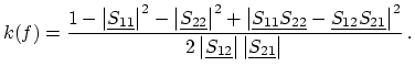 |
(3.12) |
Therefore,
![]() is the maximum frequency at which the transistor still
provides a power gain [189]. An ideal oscillator would still be
expected to operate at this frequency, hence the name maximum
oscillation frequency. Like the short-circuit current gain
is the maximum frequency at which the transistor still
provides a power gain [189]. An ideal oscillator would still be
expected to operate at this frequency, hence the name maximum
oscillation frequency. Like the short-circuit current gain
![]() ,
, ![]() drops with a slope of
drops with a slope of ![]() dB/dec.
dB/dec.
The second way to determine
![]() , which is not entirely correct
[189], is based on the maximum available gain (MAG) and the
maximum stable gain (MSG). Whereas MAG shows no definite slope, MSG
drops with
, which is not entirely correct
[189], is based on the maximum available gain (MAG) and the
maximum stable gain (MSG). Whereas MAG shows no definite slope, MSG
drops with ![]() dB/dec.
dB/dec.
![]() does not have to be necessarily larger than
does not have to be necessarily larger than
![]() . Generally,
transistors have useful power gains up to
. Generally,
transistors have useful power gains up to
![]() , that above they cannot be
used as power amplifiers any more. However, the importance of
, that above they cannot be
used as power amplifiers any more. However, the importance of
![]() and
and
![]() depends on the specific application. Thus, there is no general answer whether
depends on the specific application. Thus, there is no general answer whether
![]() should be priorized over
should be priorized over
![]() . Both figures should be as high as
possible, and manufactures often strive for
. Both figures should be as high as
possible, and manufactures often strive for
![]() in order to
enter many different markets for their transistors [189].
in order to
enter many different markets for their transistors [189].
![\includegraphics[width=8.0cm]{figures/TwoPortY2.eps}](img566.png)
![\includegraphics[width=8.0cm]{figures/TwoPortS2.eps}](img577.png)
![\includegraphics[width=10.8cm]{figures/SparamDef2.eps}](img588.png)