As already discussed above, by using the standard single-mode AC a general complex-valued amplitude can be applied to an arbitrary number of terminals of the device. However, under these circumstances the calculation and assembly of the complete admittance matrix is a cumbersome task. For that reason the simulator has been extended to provide a feature for the automatic calculation of the complete matrix.
The intrinsic scattering matrix
![]() can be calculated by the following
analytical formula [244]:
can be calculated by the following
analytical formula [244]:
| (3.20) |
 |
(3.21) |
 |
(3.22) |
| (3.23) |
| (3.24) | |
| (3.25) | |
| (3.26) | |
| (3.27) |
The capacitances are calculated according to the charge-based capacitance model [9]: the terminal charges are in general a function of the terminal voltages. Each terminal has a capacitance with respect to the remaining terminals. For that reason a four terminal device has 16 capacitances.
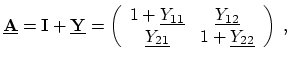
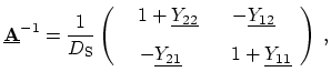
All capacitances form the so-called indefinite admittance matrix. Each element
![]() of this matrix describes the dependence of the charge at the terminal
of this matrix describes the dependence of the charge at the terminal
![]() with respect to the voltage applied at the terminal
with respect to the voltage applied at the terminal ![]() with all other
voltages held constant. In general,
with all other
voltages held constant. In general,
 |
(3.28) |
The signs are chosen to keep the capacitances positive for all devices for
which the node charge is directly proportional to the voltage at the same node,
but indirectly proportional to the voltage of any other node. Thus, for a four
terminal MOS transistor the 16 capacitances of the matrix ![]() are
defined as follows:
are
defined as follows:
![$\displaystyle C_{ij} = \left[ \begin{array}{rrrr} C_\mathrm{GG} & -C_\mathrm{GD...
...rm{BG} & -C_\mathrm{BD} & -C_\mathrm{BS} & C_\mathrm{BB} \end{array} \right]\ .$](img678.png) |
(3.29) |
Each row and column sum must be zero
in order to fulfill Kirchhoff's laws. For that reason, the capacitances
are not independent from each other, but one of the four can be calculated with
the remaining three. The gate capacitance
![]() is therefore:
is therefore:
| (3.30) |
The extended small-signal features have been evaluated by a comparison with
results of the commercial simulator DESSIS [111]. The structure,
which has been designed with the program MDRAW, was converted by using
ISE2PIF and is shown in Figure 3.11. For ![]() MHz,
MHz,
![]() , and
, and
![]() the simulator calculates
the admittance matrix shown in Table 3.1.
the simulator calculates
the admittance matrix shown in Table 3.1.
The last row of Table 3.1 contains the column sums, and the last
column the row sums. Due to numerical reasons, zero can hardly be obtained, but
the error is significantly lower than the entries in the matrix. After the
calculation of the steady-state operating point, the solution of the complex-valued
linear equation system requires 4.2![]() s on a 2.4
s on a 2.4![]() GHz Intel Pentium IV with
1
GHz Intel Pentium IV with
1![]() GB memory running under Suse Linux 8.2. The dimensions of
the complete and inner equation system are 6,610 and 4,805, respectively. In
Figure 3.12, the gate drain capacitance
GB memory running under Suse Linux 8.2. The dimensions of
the complete and inner equation system are 6,610 and 4,805, respectively. In
Figure 3.12, the gate drain capacitance
![]() as
calculated by MINIMOS-NT is compared with results of DESSIS. Note, that the
sign of the DESSIS result had to be inverted.
as
calculated by MINIMOS-NT is compared with results of DESSIS. Note, that the
sign of the DESSIS result had to be inverted.
![\includegraphics[width=0.48\linewidth]{figures/smac-compare-cgd.col.eps}](img687.png)
|
![\includegraphics[width=\linewidth]{figures/Struct1r.eps}](img684.png)