


Next: 8. Summary and Conclusions
Up: 7. Case Studies
Previous: 7.3 6T SRAM Cell
Subsections
Figure 7.22:
Circuit of a five stage ring oscillator. It consists of five CMOS
inverters with coupled in- and outputs. NBT stress mainly affects the
p-channel transistors.
|
|
In this section a five stage CMOS ring oscillator, as depicted in
Figure 7.22, is investigated with regard to NBTI degradation. A
ring oscillator comprises of an odd number of CMOS inverters. The output of
each inverter is used as input for the next one. The last output is fed back
to the first inverter. Because of the delay time of each stage the whole
circuit spontaneously starts oscillating at a certain frequency. The frequency
 depends on the number of stages
  and the delay time of the inverters
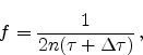
 as follows
 |
(7.3) |
Figure 7.23:
Transient oscillation in the simulation run. The circuit oscillates
with a frequency of  MHz.
MHz.
|
|
In the simulation the initial condition for the node voltages
 -
- has to be defined. In the first time step the
voltages at node N1, N3, and N4 are forced to
has to be defined. In the first time step the
voltages at node N1, N3, and N4 are forced to  V and the others to
 V. The voltages quickly reach their oscillation voltages.
Figure 7.23 shows the transient oscillation of the
inverter. This non-degraded circuit oscillates with a frequency of
 MHz. Using (7.3) the delay time of the inverters
calculates as
MHz. Using (7.3) the delay time of the inverters
calculates as  ns.
ns.
7.4.1 Frequency Degradation
Negative bias temperature instability mainly affects the p-channel transistors
in the inverter circuits. Their level of degradation is approximately equal
because of the identical stress conditions in the oscillating circuit.
NBTI leads to an increased absolute threshold voltage,
 . This, in
turn, reduces the gate overdrive required to turn on the p-channel transistors.
When turning the transistor off, on the other hand side, the overdrive is
increased and this process is therefore performed faster, as shown in
Section 7.2.3. Still, as the lower turn-on speed dominates, the
inverter's delay time increases,
. This, in
turn, reduces the gate overdrive required to turn on the p-channel transistors.
When turning the transistor off, on the other hand side, the overdrive is
increased and this process is therefore performed faster, as shown in
Section 7.2.3. Still, as the lower turn-on speed dominates, the
inverter's delay time increases,
 ,
,
 |
(7.4) |
reducing the oscillation frequency.
Figure 7.24:
Influence of NBTI on a CMOS ring oscillator. Because of the
threshold voltage shift due to NBT stress the circuit's oscillation frequency
is reduced.
|
|
Figure 7.24 depicts the oscillation voltage of the unstressed circuit
and after degradation due to NBTI. A clear reduction of the oscillation
frequency can be observed. With a very large interface degradation
 the oscillation frequency is reduced from MHz to
 MHz. The delay time of the five inverters is increased by
 ns.
ns.
Figure 7.25:
Frequency degradation versus
 . As predicted by
(7.4) the frequency of the ring oscillator is drastically
reduced with increasing NBTI degradation.
. As predicted by
(7.4) the frequency of the ring oscillator is drastically
reduced with increasing NBTI degradation.
![\includegraphics[width=0.495\textwidth]{figures/f-vs-nit}](img684.png)
Linear scale
|
![\includegraphics[width=0.495\textwidth]{figures/f-vs-nit-log}](img685.png)
Logarithmic scale
|
|
The evolution of the frequency with NBTI induced interface trap generation can
be seen in Figure 7.25. Increasing degradation leads to a reduced
oscillation frequency of the ring oscillator, as predicted by
(7.4).
To evaluate the effect of long time NBT stress on the ring oscillator's
frequency degradation a transient NBTI simulation of a single p-channel MOSFET
has been performed. Figure 7.26 shows the resulting interface trap
density
at constant voltage and constant temperature stress for 10 years
using the new model. When assuming a frequency degradation of 5% to be
within the circuits design rules, Figure 7.26(a) shows very well
that at temperatures above 100^C and with a stress voltage of
 V
the degradation exceeds this limit within 10 years (
V
the degradation exceeds this limit within 10 years ( s). At
regular operating voltage with
s). At
regular operating voltage with
 V the degradation limit is not
reached.
V the degradation limit is not
reached.
It has to be considered, though, that for these simulations constant stress was
assumed. As shown in Chapter 6 NBTI has a recovery effect when the stress
conditions are removed. Therefore, Figure 7.27 gives the resulting
degradation at periodic stress with 1Hz oscillation frequency for 1 hour. It
is not possible to simulate the whole 10 years of lifetime, as for each second
at least two simulations have to be performed, but the trend is clear. The
overall degradation is reduced for periodic stress voltages and stays below the
degradation at permanent stress conditions. This enhances the lifetime as
defined above considerably.
The same simulations have been performed using the standard reaction-diffusion
model (Figure 7.28 and 7.29). The estimated
degradation after 10 years stress is clearly different and even lies beyond the
5% border for all temperatures and voltages. This result emphasizes how
important the use of a correct model and the right model parameters is for long
time predictions.
Figure 7.26:
p-channel MOSFET degradation simulation at constant NBT stress for
10 years using the new model. A 5 % frequency degradation of the ring
oscillator is observed at
 cm
cm . Only at
(a) 25 V gate stress and more than 100
. Only at
(a) 25 V gate stress and more than 100 C the degradation threshold is
reached within 10 years. At regular operating voltage (b) the frequency
degradation stays within 5 % in 10 years.
C the degradation threshold is
reached within 10 years. At regular operating voltage (b) the frequency
degradation stays within 5 % in 10 years.
|
|
Figure 7.27:
p-channel MOSFET degradation simulation at dynamic NBT stress for 1
hour using the new model. The stress voltage oscillates with 1 Hz and a
duty cycle of 50 % (dashed lines) and with constant stress (solid lines)
have been used. The level of degradation with oscillating stress is always
below constant stress and increases the lifetime.
|
|
Figure 7.28:
p-channel MOSFET degradation simulation at constant NBT stress for
10 years using the standard reaction-diffusion model. The simulation shows
how crucial the use of the correct model is for long time predictions. The
R-D model predicts that the ring oscillator would hardly reach the 5 %
degradation within 10 years even at the harshest stress conditions.
|
|
Figure 7.29:
p-channel MOSFET degradation simulation at dynamic NBT stress for 1
hour using the reaction-diffusion model.
|
|
Next: 8. Summary and Conclusions
Up: 7. Case Studies
Previous: 7.3 6T SRAM Cell
R. Entner: Modeling and Simulation of Negative Bias Temperature Instability
![\includegraphics[width=16cm]{figures/ringosc-circuit}](img667.png)
![\includegraphics[width=16cm]{figures/ringosc-transient-oscillation}](img670.png)
![\includegraphics[width=16cm]{figures/ringosc-shift}](img680.png)
![\includegraphics[width=0.495\textwidth]{figures/single-vg25-duty100}](img688.png)
![\includegraphics[width=0.495\textwidth]{figures/single-vg5-duty100}](img689.png)
![\includegraphics[width=0.495\textwidth]{figures/single-vg25-duty50}](img690.png)
![\includegraphics[width=0.495\textwidth]{figures/single-vg5-duty50}](img691.png)
![\includegraphics[width=0.495\textwidth]{figures/single-rd-may-vg25-duty100}](img692.png)
![\includegraphics[width=0.495\textwidth]{figures/single-rd-may-vg5-duty100}](img693.png)
![\includegraphics[width=0.495\textwidth]{figures/single-rd-may-vg25-duty50}](img694.png)
![\includegraphics[width=0.495\textwidth]{figures/single-rd-may-vg5-duty50}](img695.png)