Our numerical model is applied to study the performance of thin-oxide
submicrometer MOSFETs with an (implanted) nondegenerate gate. In the first
example we analyze the threshold voltage instabilities due to gate depletion
in a small 
 -gate/-channel device with very thin oxide
 . The device has an ideal threshold voltage of
  and
is designed for room-temperature operation. Implanted source and drain
profiles are reconstructed from the data in the
literature [512][351][93][60] (see
also [472][301]). We simulated static characteristics in the
linear and the saturation region, transconductance, breakdown voltage and
threshold-voltage variation with channel metallurgical length for this device.
The results correspond to typical values reported for such experimental devices
in literature. Possible B-penetration in -gate devices is neglected in
this study (Section 2.1.2). The numerically calculated
threshold voltage
and
is designed for room-temperature operation. Implanted source and drain
profiles are reconstructed from the data in the
literature [512][351][93][60] (see
also [472][301]). We simulated static characteristics in the
linear and the saturation region, transconductance, breakdown voltage and
threshold-voltage variation with channel metallurgical length for this device.
The results correspond to typical values reported for such experimental devices
in literature. Possible B-penetration in -gate devices is neglected in
this study (Section 2.1.2). The numerically calculated
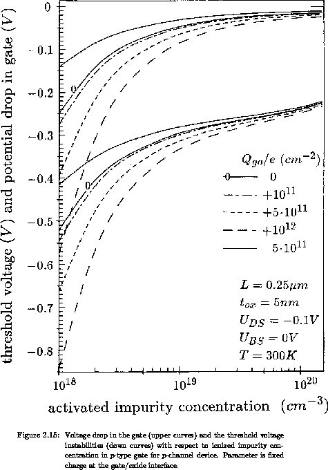
threshold voltage  and the voltage drop in the gate in the middle of
the channel
and the voltage drop in the gate in the middle of
the channel  are presented in Figure 2.15, with the
fixed charge at the gate/oxide interface
are presented in Figure 2.15, with the
fixed charge at the gate/oxide interface  being a parameter. As already
shown in Figure 2.5, a positive reduces threshold
voltage increasing due to factor in
being a parameter. As already
shown in Figure 2.5, a positive reduces threshold
voltage increasing due to factor in  -gate/-channel devices.
However, in -gate/-channel devices, a positive increases
-gate/-channel devices.
However, in -gate/-channel devices, a positive increases  and consequently, becomes larger because of an increased .
Moreover, the threshold voltage sensitivity with respect to the activated
impurity concentration
and consequently, becomes larger because of an increased .
Moreover, the threshold voltage sensitivity with respect to the activated
impurity concentration  increases with presence of a positive
in -gate/-channel devices, as shown in Figure 2.15.
Contrary to -gate/-channel devices in conventional -gate/-channel
devices the gate enters into accumulation and the influence of lowering
and positive on the threshold voltage is much weaker.
Note that B-penetration would shift to more positive values in
Figure 2.15 as opposed to a roll-off in due to
gate depletion.
increases with presence of a positive
in -gate/-channel devices, as shown in Figure 2.15.
Contrary to -gate/-channel devices in conventional -gate/-channel
devices the gate enters into accumulation and the influence of lowering
and positive on the threshold voltage is much weaker.
Note that B-penetration would shift to more positive values in
Figure 2.15 as opposed to a roll-off in due to
gate depletion.
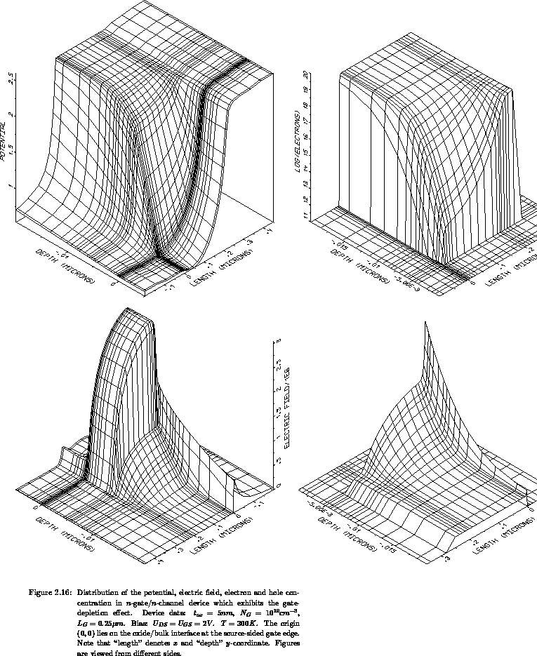
Figure 2.16 shows the distributions of potential,
electric field strength and carrier concentration in a small
-gate/-channel device, including gate, oxide and bulk area. A device
with , very thin oxide of and  is designed according to data for the technological processes,
multiple-implanted doping profiles and terminal characteristics in the
literature [512][394][393][351][93][60].
Because of the thin oxide (
is designed according to data for the technological processes,
multiple-implanted doping profiles and terminal characteristics in the
literature [512][394][393][351][93][60].
Because of the thin oxide ( ), the moderate doping in the gate
(
), the moderate doping in the gate
( ) and the high gate bias (
 ) a remarkable potential
drop occurs in the gate. The effective gate bias at the source
channel-end
) a remarkable potential
drop occurs in the gate. The effective gate bias at the source
channel-end  is reduced by
  or about
  .
.
When  is small, the gate-bias reduction
  is uniform along
the channel. In saturation, the fields
is uniform along
the channel. In saturation, the fields  and reduce when going from
source towards the drain
and reduce when going from
source towards the drain
channel-end.  decreases along the
gate/oxide interface. As a consequence, one may expect that the gate-depletion
effect becomes less important in the saturation than in the linear region; for
instance a reduction in
decreases along the
gate/oxide interface. As a consequence, one may expect that the gate-depletion
effect becomes less important in the saturation than in the linear region; for
instance a reduction in  should be smaller in the saturation
region than that in the linear region. However, a careful analysis shows that
different effects take place which tend to cancel each other out. These effects
are discussed in the following, applying the results known from analytical
MOSFET modeling and supporting the conclusions by numerical simulation
necessary for such short-channel devices.
should be smaller in the saturation
region than that in the linear region. However, a careful analysis shows that
different effects take place which tend to cancel each other out. These effects
are discussed in the following, applying the results known from analytical
MOSFET modeling and supporting the conclusions by numerical simulation
necessary for such short-channel devices.
The potential distribution along the channel in an MOSFET is a concave function
of the  -coordinate. Let us denote
  the channel potential due to
nonzero with respect to potential in the source at the gate edge. In
short-channel MOS transistors the channel potential is a slowly varying
function of the -coordinate in the source channel-part and increases rapidly
when approaching the characteristic pinch-off point (where
the channel potential due to
nonzero with respect to potential in the source at the gate edge. In
short-channel MOS transistors the channel potential is a slowly varying
function of the -coordinate in the source channel-part and increases rapidly
when approaching the characteristic pinch-off point (where
 increases enormously, [204]). In contrast,
in long-channel MOSFETs increases with a moderate slope along the whole
channel. Such a peculiarity of in short-channel devices is a
direct consequence of the non-linearity and saturation in the
increases enormously, [204]). In contrast,
in long-channel MOSFETs increases with a moderate slope along the whole
channel. Such a peculiarity of in short-channel devices is a
direct consequence of the non-linearity and saturation in the  relationship [162][161]. Therefore,
  decreases weakly
from its maximal value at the source-side when approaching the pinch-off point
near the drain-side, as can be seen on the potential and field distributions in
the gate shown in Figure 2.16. In this example, we employed a
standard drift-diffusion transport model with
decreases weakly
from its maximal value at the source-side when approaching the pinch-off point
near the drain-side, as can be seen on the potential and field distributions in
the gate shown in Figure 2.16. In this example, we employed a
standard drift-diffusion transport model with  for Si and obtain
 and
and  in the middle of the channel (
 ).
Simulating the same example, but without accounting for the drift velocity
saturation (constant mobility) is equivalent to assuming a classical
long-channel MOSFET theory. In the latter case we obtain
).
Simulating the same example, but without accounting for the drift velocity
saturation (constant mobility) is equivalent to assuming a classical
long-channel MOSFET theory. In the latter case we obtain  and
and
 at the middle of the channel for the same device.
These numerical results are consistent with our preceding discussion. In both,
the ``long'' and the short-channel device, and are
approximately the same at the source and drain-end of the channel, but they
differ within the channel due to linear and non-linear relations.
According to this finding the degradation of in saturation should be
lower, but close to that in the linear region, since depletion occurs in a
significant part of the gate for transistors biased in saturation.
at the middle of the channel for the same device.
These numerical results are consistent with our preceding discussion. In both,
the ``long'' and the short-channel device, and are
approximately the same at the source and drain-end of the channel, but they
differ within the channel due to linear and non-linear relations.
According to this finding the degradation of in saturation should be
lower, but close to that in the linear region, since depletion occurs in a
significant part of the gate for transistors biased in saturation.
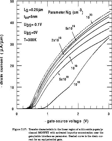
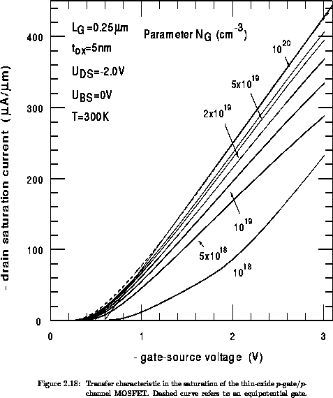
Figures 2.17 and 2.18 display the
numerically calculated drain current in linear and saturation region for the
-gate/-channel device, with activated concentration in the gate as
parameter. The numerical calculation is carried out employing the classical
drift-diffusion model with parameters for the field-dependent mobility as
in [417], being aware of all shortcomings of such an approach to
simulate  -devices biased in saturation. Calculations show that
the reduction of is always larger in the saturation than in the linear
region, contrary to our previous conclusion.
-devices biased in saturation. Calculations show that
the reduction of is always larger in the saturation than in the linear
region, contrary to our previous conclusion.
To explain this finding remember that the drain current is given by
with  representing the inversion-layer charge and
  an average
drift velocity across the inversion layer at the coordinate . It is known
that
an average
drift velocity across the inversion layer at the coordinate . It is known
that  close to the source channel-end, denoted as
  , is the main
quantity depending on
, is the main
quantity depending on  which determines the drain current in a
short-channel MOSFET. G.C.A. is best fulfilled at the source channel-end.
On the other hand the drift velocity at the source channel-end
which determines the drain current in a
short-channel MOSFET. G.C.A. is best fulfilled at the source channel-end.
On the other hand the drift velocity at the source channel-end  depends primarily on the drain-source bias . In the linear region,
 holds, where
  is the low-field
surface mobility dependent on the transversal field
is the low-field
surface mobility dependent on the transversal field  . The lowering of is determined by the
product
. The lowering of is determined by the
product  . Gate depletion reduces , but leads
to an increase in , since the depletion in the gate reduces
. The latter effect cancels the lowering
of due to in a significant amount.
. Gate depletion reduces , but leads
to an increase in , since the depletion in the gate reduces
. The latter effect cancels the lowering
of due to in a significant amount.
This explanation correlates with the numerical calculation carried out assuming
a surface mobility independent of the perpendicular field . For example in
Figure 2.17 we obtain the relative reduction of
 ,
,  and
and  for
for  ,
,  and
and
 at
at  ,
,  , respectively. In
Figure 2.17, the corresponding reduction was
, respectively. In
Figure 2.17, the corresponding reduction was  ,
,  and
and  , respectively. The differences between these two data sets arise
due to the
, respectively. The differences between these two data sets arise
due to the  effect.
In the saturation region, approaches the non-linear part of the
relationship in our device. It is accepted that the saturation
velocity  does not change with the transversal field, which is also
assumed in the mobility model employed in the numerical simulation. The drift
velocity at the source channel-end is slightly affected by
through the weak dependence
does not change with the transversal field, which is also
assumed in the mobility model employed in the numerical simulation. The drift
velocity at the source channel-end is slightly affected by
through the weak dependence  . In short-channel transistors, the
variation of with
. In short-channel transistors, the
variation of with  is small in the saturation region due to the
non-linearity and the saturation in the relation. Remember that this
effect leads to linearization in the transfer characteristic and the saturation
of transconductance in the saturation region. Moreover,
is small in the saturation region due to the
non-linearity and the saturation in the relation. Remember that this
effect leads to linearization in the transfer characteristic and the saturation
of transconductance in the saturation region. Moreover,  is practically
independent of the gate bias at the source channel-end. As a conclusion, the
lowering of in saturation is for the most part determined by the large
reduction in . This is compensated with a slight increase in
(
is practically
independent of the gate bias at the source channel-end. As a conclusion, the
lowering of in saturation is for the most part determined by the large
reduction in . This is compensated with a slight increase in
( to
to  in our example) which represents a second order effect.
Employing the analytical model from Section 2.2 to a
MOS capacitor which is equivalent to our -gate/-channel device, the
degradation in is calculated to be
in our example) which represents a second order effect.
Employing the analytical model from Section 2.2 to a
MOS capacitor which is equivalent to our -gate/-channel device, the
degradation in is calculated to be  , and
, and  for
, and at
for
, and at  ,
respectively.
These results should be compared with the lowering of
in Figure 2.18:
,
respectively.
These results should be compared with the lowering of
in Figure 2.18:  ,
,  and
and  for the same
impurity concentrations in the gate, respectively. In addition, distributions
of the surface electron concentration
for the same
impurity concentrations in the gate, respectively. In addition, distributions
of the surface electron concentration  resulting from the numerical
calculation confirm the above conclusion.
resulting from the numerical
calculation confirm the above conclusion.
In general, the degradation of is larger than the reduction of in
saturation, while the latter effect is larger than lowering of in linear
region.
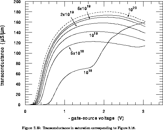
A high concentration of holes in the gate close to the source-sided gate corner
may be observed in the 2D distribution shown in Figure 2.16.
For this device the inversion in the gate takes place at  beginning at the corner. This effect produces a recovery of transconductance
to the value for equipotential-gate device, as shown in
Figure 2.19 and reported in experiments [281][226].
The gate inversion is responsible for the eccentricity in the characteristics
in Figures 2.17 and 2.18, as well.
Note that the maximum transconductance of
beginning at the corner. This effect produces a recovery of transconductance
to the value for equipotential-gate device, as shown in
Figure 2.19 and reported in experiments [281][226].
The gate inversion is responsible for the eccentricity in the characteristics
in Figures 2.17 and 2.18, as well.
Note that the maximum transconductance of  is much lower than
the ideal limit of
is much lower than
the ideal limit of  for the device
in Figure 2.19 .
for the device
in Figure 2.19 .
With regard to the influence of the charge at the gate/oxide interface
on the drain current, the numerical study has provided the result which is
consistent with that obtained for ; see Figure 2.6.
One family of the transfer characteristic is presented in [163].
Here we only repeat that has a second order influence on and
that is the main parameter determining the degradation.