to the BLs of
the arrays, the desired switching (Step 2 in Table 4.1 and Table 4.2) is enforced in the output
MTJ.
to the BLs of
the arrays, the desired switching (Step 2 in Table 4.1 and Table 4.2) is enforced in the output
MTJ.
Fig. 5.2 shows two STT-MRAM arrays which are connected in series. In the logic mode, the access
transistors of the 1T/1MTJ cells are used to select simultaneously two STT-MTJs (inputs) in one array and
one STT-MTJ (output) in the other array. Due to the serial connection of the arrays, the current flowing
through the output MTJ has a reverse polarity direction compared to the input MTJs. This means that, for
example, if the current flowing through the output MTJ tends to enforce an AP–to–P switching, the current
flowing through the input MTJs is in the P–to–AP switching direction. Therefore, the three simultaneously
selected MTJs (two inputs and one output) form the circuit topology required for the two-input
reprogrammable gate shown in Fig. 4.18a. By applying the voltage difference to the BLs of
the arrays, the desired switching (Step 2 in Table 4.1 and Table 4.2) is enforced in the output
MTJ.
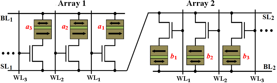
| Figure 5.2.: | Proposed STT-MRAM-based reprogrammable logic architecture including two common STT-MRAM arrays connected in series. |
Depending on the specified basic logic operation (AND, OR, NAND, or NOR),  has to be optimized as
shown in Fig. 4.20. A corresponding preset (Step 1) is performed in the output MTJ beforehand, by selecting
the desired access transistor and applying the write current/voltage signal to the BL and SL of the output
array, like in the common write operations in the memory mode. Compared to the MTJ-based
reprogrammable circuits (Fig. 4.18a and Fig. 4.18b), which require extra wiring for generating a
current-induced Oersted field for independent access to the input MTJs [55], the STT-MRAM-based
implementation enables independent STT writing of the input MTJs by using the access transistors. This
brings significant advantages related to scalability and energy consumption. However, the non-zero ON
resistance of the access transistors decreases the effective TMR ratio of the 1T/1MTJ cells by
about 10% [191]. According to Fig. 4.21, this increases the average error probabilities by a factor
of
has to be optimized as
shown in Fig. 4.20. A corresponding preset (Step 1) is performed in the output MTJ beforehand, by selecting
the desired access transistor and applying the write current/voltage signal to the BL and SL of the output
array, like in the common write operations in the memory mode. Compared to the MTJ-based
reprogrammable circuits (Fig. 4.18a and Fig. 4.18b), which require extra wiring for generating a
current-induced Oersted field for independent access to the input MTJs [55], the STT-MRAM-based
implementation enables independent STT writing of the input MTJs by using the access transistors. This
brings significant advantages related to scalability and energy consumption. However, the non-zero ON
resistance of the access transistors decreases the effective TMR ratio of the 1T/1MTJ cells by
about 10% [191]. According to Fig. 4.21, this increases the average error probabilities by a factor
of  . Therefore, MTJs with higher TMR ratio are required to compensate the reliability
decrease.
. Therefore, MTJs with higher TMR ratio are required to compensate the reliability
decrease.
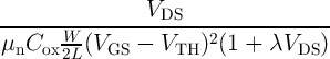
The effect of the channel resistances of the access transistors ( ) can be taken into account by using the
following equations [193]:
) can be taken into account by using the
following equations [193]:
 (
( ) is the voltage difference between the gate (drain) and the source of the access transistor,
  denotes the mobility of electrons,
  indicates the gate oxide capacitance per unit area,
  (
( )
represents the channel width (length), and
)
represents the channel width (length), and  is the channel-length modulation coefficient in saturation
(
is the channel-length modulation coefficient in saturation
( ).
).
For the STT-MRAM-based reprogrammable implementation of more complex Boolean logic
functions, a sequence of basic logic operations including AND, OR, NAND, and NOR has to be
constructed. As an example, we consider the implementation of the exclusive OR (XOR) function
which is a fundamental logic function in arithmetic circuits. The output of the XOR function
( ) is logic ‘1’, if ONLY one of the inputs is ‘1’ and can be expressed as
‘
) is logic ‘1’, if ONLY one of the inputs is ‘1’ and can be expressed as
‘ ’ or ‘
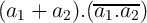 ’. It can be shown that the design based on the last expression requires
a minimum of sequential steps (6 steps) for implementation using the STT-MRAM arrays as
follows:
’. It can be shown that the design based on the last expression requires
a minimum of sequential steps (6 steps) for implementation using the STT-MRAM arrays as
follows:
| Preset : | b1 = 1 | ||
| OR : | b1 = a1 + a2 | ||
| Preset : | b2 = 0 | ||
| NAND : | b2 = a1.a2 | ||
| Preset : | a3 = 1 | ||
| AND : | a3 = b1.b2 ≡ a1 ⊕ a2 ≡ a1 XOR a2. | (5.2) |
 and
and  are the logic variables equivalent to the resistance states of the MTJs in the Array 1 and
Array 2, respectively (Fig. 5.2).
are the logic variables equivalent to the resistance states of the MTJs in the Array 1 and
Array 2, respectively (Fig. 5.2).  and
and  are the input variables stored in two MTJs in the Array 1 and
the final result (
are the input variables stored in two MTJs in the Array 1 and
the final result ( ) is written in an MTJ in Array 1. There are two intermediate basic operations on
  and
and  (OR and NAND), the respective results (
 and
and  ) are stored in two arbitrary MTJs in Array 2
for performing the final basic operation (AND).
) are stored in two arbitrary MTJs in Array 2
for performing the final basic operation (AND).  and
and  are the inputs of the final operation and Array 2
(Array 1) acts as the input (output) array.
are the inputs of the final operation and Array 2
(Array 1) acts as the input (output) array.
As the output of one operation can be used as the input data for the next logic stage, complex Boolean logic functions are designed by executing a well defined set of subsequent basic operations. Furthermore, the MTJs can be selected arbitrarily (two in the input array and one in the output array). The computation framework in the STT-MRAM architecture is flexible and not localized like in the MTJ circuits shown in Fig. 4.18 and Fig. 4.12. MRAM-based logic not only extends the functionality of the STT-MRAM architecture to perform non-volatile logic, but also eliminates the need for data transfer between separated memory and logic units which allows to shift away from the Von Neumann architecture and to shorten the interconnection delay.
By assuming the optimized  for each basic operation, we use the minimum
  values (Fig. 4.20) for
calculating
values (Fig. 4.20) for
calculating  . For example, by using Eq. 4.27 and Fig. 4.21 for
  , the average error
probability of the XOR function described in Eq. 5.2 is obtained as
, the average error
probability of the XOR function described in Eq. 5.2 is obtained as
 | (5.3) |
For the sake of higher reliability, one can design a complex logic function based solely on the AND and NAND operations, as these are more reliable compared to the OR and NOR operation in the reprogrammable implementation. However, the reliability-based design increases the number of required basic logic operations for implementation and thus, increases the computation time and the energy consumption. For example, the reliability-based design of the XOR function requires the following steps in the reprogrammable MRAM-based logic architecture:
The average error probability of the XOR operation for this design is about  , which
is four times smaller than that of the design with minimized steps. However, the number of
sequential steps and therefore, the computation time and the energy consumption are approximately
doubled.
, which
is four times smaller than that of the design with minimized steps. However, the number of
sequential steps and therefore, the computation time and the energy consumption are approximately
doubled.
![----------[------VDS----------------]-
W-- VD2S-
μnCox L (VGS - VTH )VDS - 2](diss1062x.png)