For deep-sub-micron semiconductor process technology, the use of Polysilicon fuses, as one-time-programmable devices providing memories up to several kilobits offers a cheap, efficient, and area-saving alternative to small non-volatile memories for System-on-a-Chip solutions. Approaches to increase the memory density by using 3-state fuses of layered materials are also reported [185]. Another important application is the use in simple field programmable gate arrays or for trimming CMOS circuits for specific analog performance [186]. Furthermore, the fuses are used to provide variable elements as trimmable resistor or capacitor arrays [187]. Finally, the fuses may act as the classical protective elements for improved protection and replacement of critical components before actual failures [188]. Programming is performed by sending a broad current pulse through the fuse, resulting in an open-circuit after transition to a second-breakdown state. The transition occurs when parts of the Polysilicon layer reach the melting point, and the molten Silicon is transported from the negative end through drift of ions in the applied field [189]. Fuses implemented in deep sub-micron technologies become more and more attractive in terms of power and area consumption, and hybrid approaches using other materials are getting less important [190]. Nevertheless, going to smaller ground rules below 350 nm, implies decreasing supply voltages to 1.5 V and below [191]. This constraint requires a careful optimization of the fuse layout, ensuring an efficient and reliable programming mechanism [192] and minimizing the necessary power consumption of the fusing process. As the fusing process takes place in a short time interval (between a couple of nanoseconds up to the microsecond range), direct thermal measurements of this process are quite hard to obtain. Previous work [193] already shed some light on the physics behind the fusing mechanism, but the optimization of the fuse structure for reliable and fast fusing was only possible via expensive experimental work by using test chips.
This work focuses on gaining better insight into the materials characteristics used in the structure, to enable a layout optimization through simulation. Since the electrical and thermal properties of Polysilicon are a complex function of Polysilicon film doping, grain size, and grain morphology[194], the average electrical and thermal properties as a function of temperature were obtained by experimentally measuring the transient resistivity response of the fuse through Joule self-heating, and subsequent inverse modeling the measured data, to fit the observed behavior. The electro-thermal self-heating simulations were performed with the Smart-Analysis-Package (SAP) for three-dimensional interconnect simulation [195] in combination with SIESTA, a TCAD optimization framework combining gradient based and genetic optimizers[143]. This approach enabled the optimization of the fuse layout by significantly saving costs normally spent in design and production of layout test chips. Furthermore, a better insight into the transient electro-thermal effects occurring in the first couple of microseconds was gained.
The fuse devices were fabricated in an industry-standard deep sub-micron
polycided gate CMOS process. On a specialized test chip multiple layout
variations were placed to find the optimum layout for fast and reliable
fusing. A more complicated example of a fuse structure is shown in
Figure 6.25. The first experiments were performed with rectangular
pulses. Nevertheless, through the steep slope of the fuse terminal voltage the
initial time regime of the fuse heating is not well resolved. Furthermore, the
initial transient behavior of the measurement circuit yields high errors in
the measured current data. To overcome these problems a voltage ramp was
applied and the resulting fusing resistance was calculated by assuming ohmic
behavior. The Polysilicon layer in the fuse is doped to solid solubility, and
therefore its conductivity may considered to be approximately ohmic. Since all
materials in the fuse except the Polysilicon layer are metallic, this
assumption shall give a reasonable estimate for the fuse resistivity. The
devices were stressed with different triangular voltage ramps for a few
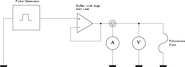
microseconds. A pulse generator was used to define the length of the pulse. As
the generator has a typical output impedance of 50
![]() and the
resistor of the Polysilicon fuse is lower than that, the source has to be
buffered by an operational amplifier with a high slew rate to get a stable
voltage. In order to avoid an additional voltage drop on a shunt resistor a
current probe was used. In addition, the voltage on the fuse was monitored by an
oscilloscope to calculate the right resistor value. The measurement principle
can be seen in Figure 6.23.
and the
resistor of the Polysilicon fuse is lower than that, the source has to be
buffered by an operational amplifier with a high slew rate to get a stable
voltage. In order to avoid an additional voltage drop on a shunt resistor a
current probe was used. In addition, the voltage on the fuse was monitored by an
oscilloscope to calculate the right resistor value. The measurement principle
can be seen in Figure 6.23.
The resulting measurement data for three different source voltages as a function of time are shown in Figure 6.24.
The resistance difference between the three voltages is caused by self heating of the
whole structure (including the contact barrier layers) in the first microsecond
of the applied pulse. The negative temperature coefficient of the resistance
in all three curves occurs through the combined Joule self-heating of the
Polysilicon/Polycide layer sandwich (see Figure 6.25).
The high noise in the data during the first
![]() originates
from the low voltage level in this time regime and the resulting low
signal-to-noise ratio.
originates
from the low voltage level in this time regime and the resulting low
signal-to-noise ratio.
| (6.5) |
 |
(6.6) |
| (6.7) |
The simulation framework SIESTA provides a wide range of optimizers that can be chosen to fit best for the current problems. Reference data for this optimization are measurements of the resistance calculated from Figure 6.24. At start time SIESTA provides the initial values of the free parameters for the three-dimensional interconnect simulator STAP of the SAP package, as introduced in [195]. The output of the simulation is parsed by SIESTA in order to compare it with the reference data. It produces a score value that indicates how good these two data sets match. This value is submitted to the optimizer which generates corresponding to the score value the next n-tuple of free parameters to improve the next score value that will be evaluated after the next simulation run with the currently produced values.
Wide interval ranges of free parameters can result in convergence problems because of non-physical parameter values which would cause negative resistance or negative doping. To avoid this, the simulation framework SIESTA provides a kind of divergence detection where SIESTA is signaled when the simulator has problems to converge. This feature allows the user to expand the intervals of the free parameters in a larger range as before.
The simulation framework SIESTA has to fit the thermal parameters of the
electrical and thermal conductivities in order to minimize the difference
between the reference and the simulation. To check the consistency of the
setup, all thermal and electrical parameters were used for the automated
simulation run, resulting in a total of 10 parameters. The best fit
to the measured reference data is given in Table 6.3. The
electrical and thermal conductivities
![]() and
and
![]() as well as the linear
temperature coefficient of the thermal conductivity
as well as the linear
temperature coefficient of the thermal conductivity
![]() for Polysilicon are
in excellent agreement with data reported in [194]. The
electrical conductivity of the Polysilicon/Tungsten Silicide sandwich as a
function of temperature is comparable to data measured electrically by external
heating of the layers.
for Polysilicon are
in excellent agreement with data reported in [194]. The
electrical conductivity of the Polysilicon/Tungsten Silicide sandwich as a
function of temperature is comparable to data measured electrically by external
heating of the layers.
|
The optimized parameter set results in resistance characteristics as shown in
Figure 6.26 where an excellent match with the measurements is obtained. The
strong increase of the resistance as a function of time because of self heating can
be clearly seen. In addition, after a certain critical temperature is reached,
the resistance drops dramatically and the ohmic approximation looses its
validity. In order to generalize this result to other fuse geometries,
this critical temperature has to be extracted. As expected,
the critical temperatures of all the three samples are inside of a small interval
about
![]() (cf. Figure 6.28).
This value is much smaller as the single
crystal Silicon melting point of
(cf. Figure 6.28).
This value is much smaller as the single
crystal Silicon melting point of
![]() and the Tungsten Silicide (WSi
and the Tungsten Silicide (WSi![]() phase)
melting point of
phase)
melting point of
![]() [199].
The maximum temperature of the Polysilicon fuse is observed in the center of the
Tungsten Silicide layer as shown in Figure 6.28.
[199].
The maximum temperature of the Polysilicon fuse is observed in the center of the
Tungsten Silicide layer as shown in Figure 6.28.
Several mechanisms for this low critical
temperature are possible. First, the disordered region between the Tungsten Silicide
and the Silicon may have a stoichiometry closer to the eutectic point of the
Tungsten-Silicide system and therefore a lower melting point. But since the lowest
eutectic temperature of the W-Si system is
![]() [199], this is not likely for pure
alloys. Second, the high doping concentration of the Polysilicon layer reduces
the melting temperature as reported for Silicon glasses with high Boron and
Phosphorus contents. Finally, the assumption that all materials show Ohmic
behavior over the full temperature range between
[199], this is not likely for pure
alloys. Second, the high doping concentration of the Polysilicon layer reduces
the melting temperature as reported for Silicon glasses with high Boron and
Phosphorus contents. Finally, the assumption that all materials show Ohmic
behavior over the full temperature range between ![]() and
and
![]() does not hold for higher temperatures.
does not hold for higher temperatures.
The intended target to optimize fuse layouts for better performance is not affected, since it is obvious from Figure 6.27 that the melting begins always at approximately the same temperature. Therefore, the method should be applicable for other geometries as well. The agreement between experiment and simulation is excellent and provides a reliable base for carrying out predictive simulations of the transient temperature distribution during the initial heating phase of the fusing.
|
![\includegraphics[origin=c,width=0.8\textwidth,clip=true]{figures/polyfuse_Temp-sim.rot.ps}](img321.png)
|
A method for obtaining important material parameters by inverse modeling using finite element simulations of complex interconnect structures was presented. This method is capable of describing the electrical behavior of interconnect materials over a significant temperature interval. Furthermore, it uses the transient thermal self-heating effect to separate different materials and their electrical and thermal properties. Nevertheless, the exact conduction mechanism inside the Polysilicon layer is still not well reflected in this analysis. In further work the impact of the grain boundary barriers and their behavior at high temperature has to be addressed by implementing a more accurate model like the model of Mandurah [200]. It was demonstrated that the method is consistent and gives an excellent match to experimental results. With the extracted critical temperature, where the material looses its ohmic properties, the geometry can be optimized in terms of reliability and speed.
![\includegraphics[origin=c,width=1.0\textwidth,clip=true]{figures/polyfuse_ramp.rot.ps}](img278.png)
![\includegraphics[origin=c,width=1.2\textwidth,clip=true]{figures/polyfuse_structure.rot.ps}](img280.png)
![\includegraphics[origin=c,width=0.8\textwidth,clip=true]{figures/polyfuse_R-sim.rot.ps}](img314.png)
![\includegraphics[angle=0,origin=c,width=1.2\textwidth,clip=true]{figures/polyfuse_temp-dist.ps}](img322.png)