![[ 2 ]
M (q) = ℏ---dΨi(z)-dΨj(z)- | Δ (q),
i,j 2ml dz dz z = ± -t
2](disser139x.png)
The interface between Si and SiO2 plays an important role in determining transport in MOSFETs. Because of non-ideality small perturbations at the interface appear, that lead to field fluctuations and contribute to the scattering. These fluctuations are of several atomic layers size due to processing. Surface roughness scattering is an important relaxation mechanism that is be accounted in MOSFETs simulations. Ultrathin sandwiched structures, where a thin silicon film is placed between two silicon oxides, are more sensitive to surface roughness scattering. Thus, the importance of the surface roughness scattering increases.
Since devices sizes become smaller and the limit of 5nm [39] film thickness after which the surface roughness starts dominating over all other scattering mechanisms achieved in near future, understanding the details of that mechanism is needed.
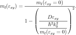
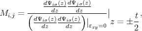
If one assumes a non-degenerate parabolic band dispersion and an infinite barrier at the silicon-oxide interface the surface roughness scattering matrix elements are proportional to the product of the subband eigenfunction derivatives at the interface [55]
|
| (6.1) |
Here, Δ(q) is the Fourier transform of the random variation of the interface position with respect to the in-plane r coordinate, q is the wavevector change due to scattering, Ψi,j are the subband eigenfunctions in a silicon film, and t is the film thickness. The generalization of this expression to the k⋅p theory when the subband functions consist of several components is required. An additional difficulty appears in strained films where the longitudinal mass is the function of shear strain
 | (6.2) |
In order to resolve the question which mass to use, an alternative approach by Esseni [29] is being followed, where the surface roughness intrasubband scattering matrix elements are
![Mi,j(q) = [ΔEC (Ψi (z ),Ψj (z))]| Δ(q).
z = ± t-
2](disser141x.png) | (6.3) |
In the limit of ΔEC →∞ Equation 6.1 and Equation 6.3 must produce the same result [55, 29].
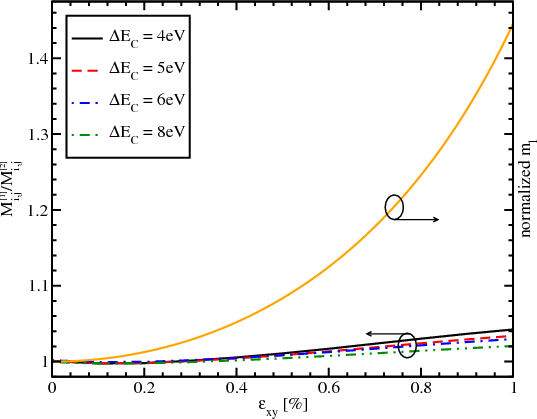
Figure 6.1 shows the dependence of the longitudinal effective mass obtained from the ratio of the surface scattering elements calculated with Equation 6.1 and Equation 6.3, for several values of ΔEC, as a function of shear strain. Also the dependence of the longitudinal effective mass normalized to the ml at zero strain on the shear strain according to Equation 6.2 is shown.
The observed effective mass obtained from the ratio of the matrix elements calculated with two different methods changes only a little with strain. These changes are becoming smaller as the conduction band offset increased. It means that the longitudinal effective mass in Equation 6.1 must not depend on shear strain. Therefore, within the k⋅p method the surface roughness scattering matrix elements are generalized as
![[ 2 ( ) ]
M (q) = -----ℏ------- dΨi(z), dΨj(z)- | Δ(q).
i,j 2ml(εxy = 0) dz dz z = ± t-
2](disser145x.png) | (6.4) |
Here, (a,b) is the scalar product between the two multi-component subband functions a and b. An expression similar to Equation 6.4 has been employed in the six-band k⋅p calculations [35].
The surface roughness induced momentum relaxation matrix elements normalized to the value of the intrasubband scattering at zero strain are then calculated as
 | (6.5) |
where σ = ±1 is the spin projection to the [001] axis.
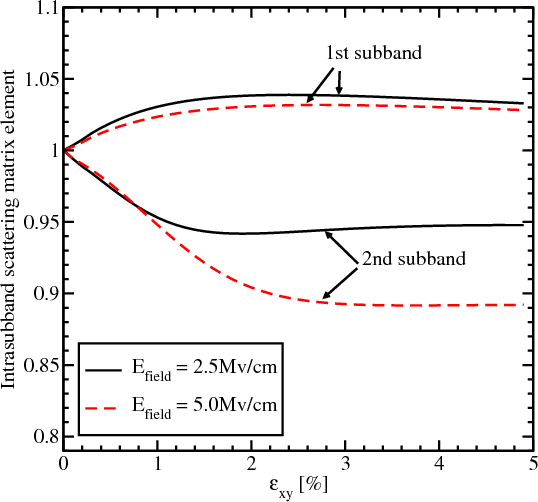
The surface roughness at the two interfaces is assumed to be equal and statistically independent. It is described by a mean and a correlation length [35]. Figure 6.2 and Figure 6.3 show the dependences on strain of the matrix elements for intrasubband and intersubband scattering normalized to the value of the intrasubband scattering at zero strain, for two values of the effective electric field. The intrasubband scattering matrix element within the lowest unprimed subband only marginally depends on shear strain. Indeed, it shows a few percent increase which becomes smaller at high shear strain, where it starts approaching unity again. This is expected in the limit of high stress. In this limit both valleys merge at the common minimum in the X point and the band dispersion is well described by a parabolic approximation [111]. Thus the lowest subband energy and the intrasubband scattering matrix element must approach their respective values in unstrained film where the dispersion is also parabolic.
The intrasubband scattering matrix element in the second subband displays a slight decrease with strain increased, which saturates at high strain. In the high strain limit the second subband, which was equivalent to the first unprimed subbands in the unstrained film, transforms into the second subband of the triangular well potential. Thus the carriers are located effectively further away from the interface. This reduces the value of the intrasubband scattering matrix elements as compared to the unstrained case, in agreement with Figure 6.2. The dependence on the electric field is explained by a slight reduction of the derivative of the wave function at the interface due to its stronger penetration under the potential barrier for higher effective fields.
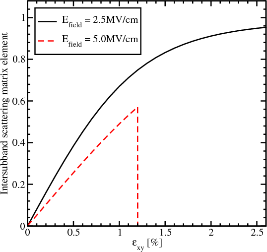
As shown in Figure 6.3, the intersubband matrix scattering element is zero in an unstrained film, in agreement with the general rule that elastic scattering does not produce transitions between the equivalent subbands originating from the opposite equivalent valleys [55]. Shear strain lifts the subband degeneracy and thus results in a sensible intersubband scattering. Because of the subband splitting, the intersubband scattering depends strongly on the kinetic energy within the lowest subband: if the kinetic energy becomes lower than the subband splitting, the scattering vanishes. The intersubband splitting is larger at stronger effective electric fields, therefore, the intersubband scattering is suppressed already at weaker strain provided the kinetic energy within the subband is the same, in agreement with Figure 6.3.
The surface roughness momentum relaxation rate is calculated in the following way [117, 29]
![∫
1 2π ∑ 2π 2 2 1 ℏ4 |Kj |
τSR-(K--)-= -----2- π Δ L ϵ2-(K----K--)4m2-||∂E--(K-)-||⋅
i i ℏ(2π ) j 0 ij i j l||-------j ||
∂Kj
[ ( dΨ ) *( dΨ ) ]2 ( - (K - K )L2 )
⋅ --iKiσ- ---jKjσ t exp -----j----i---- dφ.
dz dz z = ± -- 4
2](disser147x.png) | (6.6) |
Ki,Kj are the in-plane wave vectors before and after scattering, φ is the angle between Ki and Kj, ϵ is the dielectric permittivity, L is the autocorrelation length, Δ is the mean square value of the surface roughness fluctuations, ΨiKi and ΨjKj are the wave functions, and σ = ±1 is the spin projection to the [001] axis.
The momentum scattering relaxation rate is calculated as
![⌊ | | ⌋
∫ ||∂E-(Kj-)||f (E (K ))
1 2 πkBT ∑ 2π dϕ 1 Kj | | ∂Kj | j |
-PH------= ----2-- -------2-||∂E--|||⌈1 - ||∂E--(K--)||-----------|⌉ ⋅
τi (Ki ) ℏρυPH j 0 2π (2π) |---j| |------i-|f (E (Ki))
|∂Kj | | ∂Ki |
∫ t[ † ][ † ]
⋅ 2π Ψ jKjσ (z)M PHΨiKi σ (z) ΨjKjσ (z) M PH ΨiKiσ (z ) dz⋅
0
⋅ θ(Ei - Ej ),](disser148x.png) | (6.7) |
where υPH =  [51], and MPH is defined as
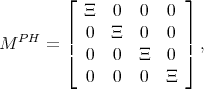 | (6.8) |
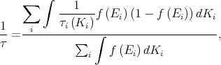
The momentum relaxation times are calculated by thermal averaging [70, 107, 35] as
 | (6.9) |
 | (6.10) |
 | (6.11) |
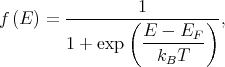
where kB is the Boltzmann constant, T is the temperature, EF is the Fermi energy, E = Ei(0) + E i(Ki), Ei(0) = E i(Ki = 0) is the energy of the bottom of the subband i, and
 | (6.12) |
is the derivative of the subband dispersion along Ki at the angle φ defining the Ki direction.
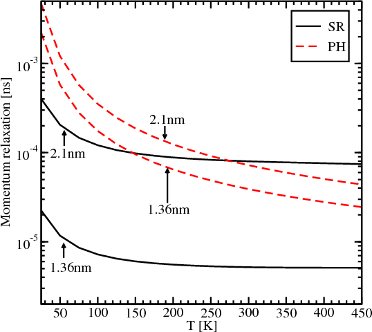
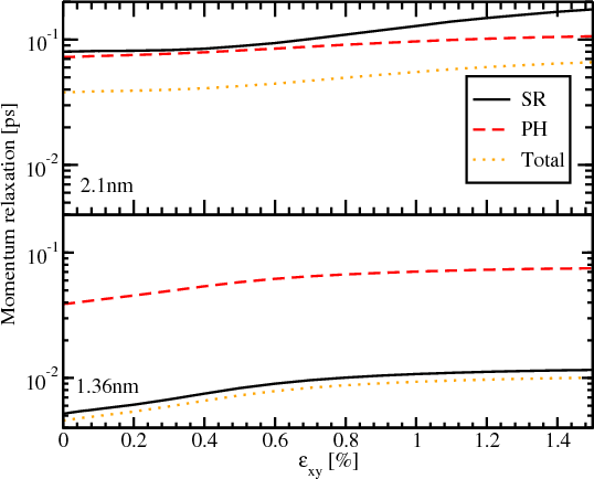
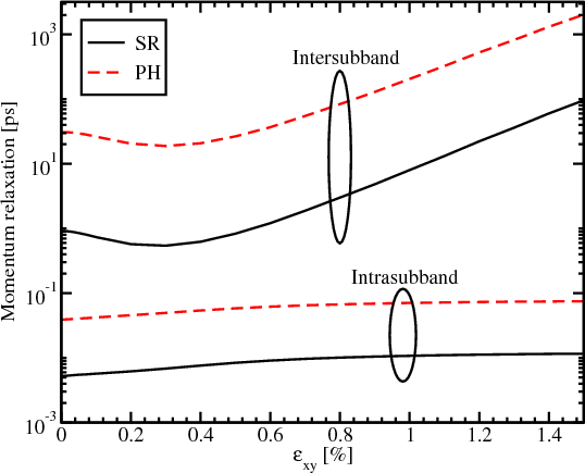
Figure 6.4 shows the dependence of the momentum relaxation time on temperature for surface roughness and acoustic phonons. For the film thicknesses 2.1nm and 1.36nm the contribution from the surface roughness is dominant at low temperatures. However, for a temperature around 280K the contributions from the surface roughness and from the acoustic phonons for the film of thickness 2.1nm are equal. Any further increase of temperature leads to higher values of the momentum relaxation time caused by acoustic phonons. Figure 6.4 illustrates that the dominant relaxation mechanism strongly depends on film thickness. The phonons limited momentum relaxation is characterized by a much weaker thickness dependence and does not change significantly when the thickness decreases from 2.1nm to 1.36nm. The surface roughness limited momentum relaxation decreases by more than an order of magnitude as expected [35, 55]. Thus, for the thickness of 1.36nm the surface roughness induced spin relaxation is the dominant mechanism for the whole range of considered temperatures.
Figure 6.5 shows the dependence of the different mechanisms of the momentum relaxation together, including the total momentum relaxation time, as a function of shear strain. The improvement of the momentum relaxation time due to the shear strain is around 82% for the film thickness of 2.1nm and around 120% for the film thicknesses 1.36nm. The acoustic phonons limited momentum relaxation improves around 45% for 2.1nm and around 92% for 1.36nm. The surface roughness limited momentum relaxation time increases around 110% for 2.1nm and around 120% for 1.36nm. Due to the dominant surface roughness mechanism for the film thickness of 1.36nm, the increase of the total momentum relaxation time is higher for 1.36nm than for 2.1nm. The increase of the momentum relaxation time is due to the corresponding scattering matrix elements dependence on strain. Combined with the strain induced transport effective mass decrease it should result in an even better mobility improvement supporting the use of uniaxial tensile strain as the mobility booster in fully depleted ultra-thin SOI FETs.
Figure 6.6 demonstrates the contribution of the inter- and intrasubband processes to the acoustic phonon and surface roughness limited momentum relaxation. The domination of the intrasubband relaxation processes for both mechanisms of the momentum relaxation is shown, in agreement with the selection rule that the elastic processes result in strong intrasubband relaxation. The dominance of the surface roughness mechanism for the film thickness 1.36nm shown in Figure 6.4 and Figure 6.5 is the consequence of the high intrasubband relaxation rate.
The electron mobility in the inversion layer in the [110] direction is calculated as [35]
 | (6.13) |
where ns = ∑ ini, ni is the population of subband i, and τ110(i) is the momentum relaxation time in subband i for [110] direction.
When more than one scattering process is considered, for example surface roughness and electron-phonon, the total mobility is calculated by Matthiessen’s rule [64, 65]
 | (6.14) |
where μ is the total mobility, μSR is the mobility due to surface roughness, and μPH is the mobility due to lattice phonons.
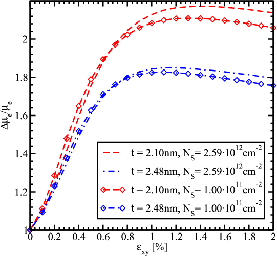
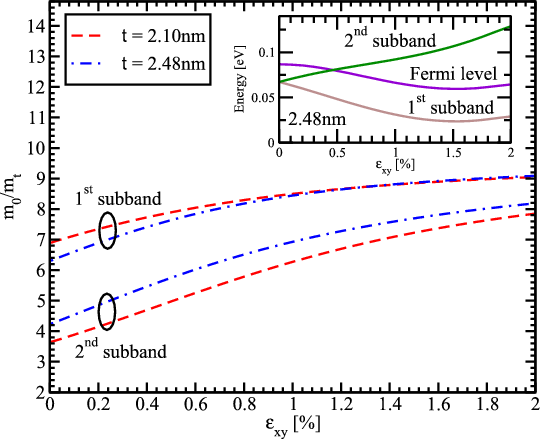
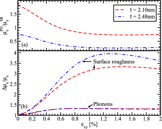
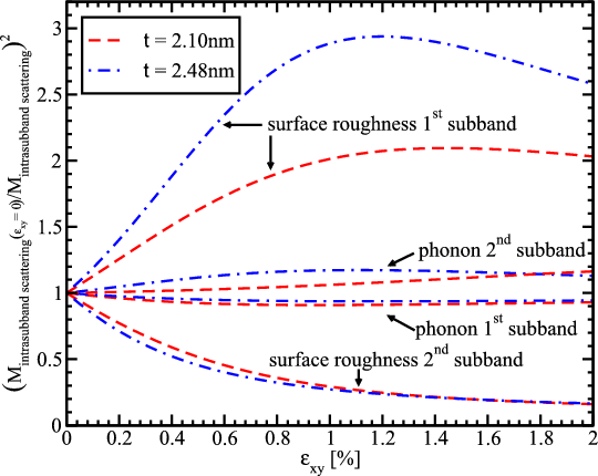
Figure 6.7 shows the electron mobility enhancement in [110] direction along tensile stress as a function of shear strain. The simulations show that the mobility in thin silicon films increases by a factor of two. The increase depends on the electron concentration and the film thickness. For the thicknesses considered a strong mobility enhancement is observed up to a shear strain value around 0.5%. When the shear strain is further increased the mobility saturates and even shows a slight decrease for the film thickness 2.1nm and 2.48nm.
The [110] mobility enhancement in surface layers due to tensile stress applied along the channel is usually explained by the effective transport mass reduction [116, 115]. However, the effective mass decrease in the lowest subband shown in Figure 6.8 may only account for roughly one half of the mobility enhancement obtained and cannot explain the two-fold mobility enhancement. Thus, a more detailed analysis is needed to understand the effect. The ratio of the phonon electron mobility to the surface roughness limited mobility as a function of strain is shown in Figure 6.9a. The surface roughness limited mobility in the 2.1nm thick film is of the same order as the phonon electron mobility. Thus, the total mobility is determined by the interplay between these two mechanisms. For the 2.48nm thick film the contribution of the phonon mobility is higher than for the 2.1nm thick film. The enhancement of the surface roughness and phonon limited mobility is shown in Figure 6.9b. The phonon mobility demonstrates an increase of about 40% consistent with the transport effective mass decrease. This behavior is supported by an almost negligible dependence of the electron-phonon scattering matrix elements on strain (Figure 6.10).
On the other hand, the surface roughness limited mobility for 2.1nm and 2.48nm thick films rises by about 200 and 300 percent, respectively, at around 1.2% shear strain and shows a slight decrease at strain values bigger than 1.2%. This behavior is dictated by the corresponding enhancement of the inverse surface roughness scattering matrix elements (Figure 6.10). The mobility enhancement shown in Figure 6.9b and their ratio shown in Figure 6.9a are consistent with the total mobility enhancement observed in Figure 6.7. Indeed, for the t=2.1nm film the unaccounted mobility enhancement is mostly due to the surface roughness limited mobility increase. Although the surface roughness limited mobility growths even stronger for t=2.48nm, the main contribution limiting the mobility is the phonon scattering. For this reason the whole mobility is slightly less enhanced as compared to that in the t=2.1nm film.