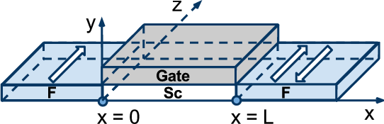
Figure 8.1: Schematic illustration of the spin field-effect transistor.
The spin field-effect transistor (SpinFET) is a future semiconductor spintronics device promising to deliver a performance superior to that achieved with present transistor technology. A schematic illustration of the SpinFET is shown in Figure 8.1. SpinFETs are composed of two ferromagnetic contacts (source and drain), which sandwich the semiconductor region. Ferromagnetic contacts contain mostly spin-polarized electrons and play the role of polarizer and analyzer as described by Datta and Das [22]. The ferromagnetic source contact injects spin-polarized electrons into the semiconductor region. Because of the non-zero spin-orbit interaction the electron spin precesses during the propagation through the channel [72, 14]. At the drain contact only the electrons with spin aligned to the drain magnetization can easily leave the channel and contribute most to the current. Thus, the total current through the device depends on the relative angle between the magnetization direction of the drain contact and the electron spin polarization at the end of the semiconductor channel. Current modulation is achieved by tuning the strength of the spin-orbit interaction in the semiconductor region and thus the degree of the spin precession. Importantly, the strength of the spin-orbit interaction in the channel depends on the effective electric field and can be controlled by the voltage applied to the gate [84, 44, 28, 101, 46, 42, 74, 129].
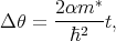
The spin precession angle Δθ defined as the difference between the orientation of the spin of the electron at the end and at the beginning of the semiconductor region is [109]
 | (8.1) |
where α is the strength of the spin-orbit interaction, m* is the effective mass of the electron, ℏ is the reduced Planck constant, and t is the length of the semiconductor channel. In the absence of spin-orbit interaction and external magnetic field the electrons propagate with their spin orientation conserved. The strength of the spin-orbit interaction determines the minimum length of the semiconductor channel, which will be required to change the orientation of the spin to its opposite direction. Therefore, a tradeoff between spin lifetime and spin-orbit strength for sufficiently short channel needs to be found. Thus, in case of a material with a strong spin-orbit interaction such as InAs the semiconductor channel will be shorter than for a material with the weaker spin-orbit interaction such as silicon.
Large spin lifetime in silicon was shown in the previous chapters. Due to the excellence experience, and vast knowledge related to silicon and CMOS technology it is very attractive to investigate spin-based switching devices with silicon as a channel material. In order to relate the performance of silicon, InAs is studied as well.
Spin transport plays the same important role in spin electronics as a charge transport in the traditional electronics. Spin-dependent scattering, spin diffusion, and spin injection through an interface, and control of the spin by magnetic field are the questions spintronics considers. Spin polarization can be achieved by optical spin excitation with circularly polarized light [91, 67, 81, 76] and a current flowing from a ferromagnetic material into a non-magnetic material [19, 77, 59].
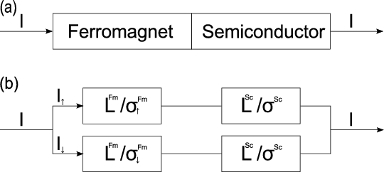
The intrinsic peculiarities of an ordinary ferromagnet lead to different conductivities for the two groups of electrons, parallel and anti-parallel to the magnetization direction of the ferromagnet. The current through the ferromagnet can be considered as spin polarized. In other words, the current of the spin up electrons (I↑) is not equal to the current of the spin-down electrons (I↓) as shown in Figure 8.2.
To effectively operate SpinFETs, the into the semiconductor injected spin-polarized current should preserve inequality between I↑ and I↓. To fulfill the condition that electrons mostly preserve their spin the transport time (τtr) should be much less compare to the spin relaxation time (τs)
 | (8.2) |
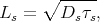
The characteristic length of spin propagation in a semiconductor is determined by [102, 37, 134, 135, 121]
 | (8.3) |
where Ds is the diffusion coefficient.
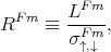
However, it is hard to achieve high spin injection efficiency in a ferromagnet/semiconductor junction. The problem is known as the conduction impedance mismatch problem [103, 109, 96, 32, 57]. The problem comes from the big difference between the semiconductor and ferromagnet conductions. Experiments [33] showed that the electrical injection of spin-polarized electrons in a semiconductor is not efficient. Authors stated that despite all their efforts, they have not been able to observe spin injection [33]. A physical explanation of that problem is given in [58, 102]. In Figure 8.2 (b) an equivalent circuit for up-down current in a ferromagnetic/semiconductor junction is shown. Each region of the junction is characterized by its own effective resistance, determined by the spin diffusion lengths in the bulk regions, or by the spin-dependent conductances in the contact [31, 60].
Following [31] the effective resistance of the ferromagnetic RFm and semiconductor RSc regions are introduced. The effective resistance is not equal to the electrical resistance of the region, it appears in the spin-polarized transport and is roughly equal to the actual resistance of the region of size LFm (LSc) [31]
 | (8.4) |
 | (8.5) |
where σ↑,↓Fm(σSc) is the conductivity of the ferromagnetic (semiconductor) region. The spin injection coefficient is determined by
 | (8.6) |
The observed low values of γ are the consequence of a big difference in conductivity between the ferromagnet and the semiconductor in the ferromagnet/semiconductor junction [102]. Indeed, if the following inequality
 | (8.7) |
is true then I↑ and I↓ are practically the same. Thus, no spin injection is observed. There are two approaches to overcome this problem: 1) instead of an metallic ferromagnet use a ferromagnetic semiconductor that has a resistivity almost equal to the resistivity of the semiconductor (R↑,↓Fm ≈ RSc); 2) use of a normal metallic ferromagnet but ensure a very high junction resistance (Rc) [96, 31]
 | (8.8) |
To fulfill Equation 8.8 a thin insulating tunnel barrier was introduced in [80]. The authors approach was to use AlOx insulator as a tunnel barrier between the ferromagnetic layer and the (AlGa)As semiconductor heterostructure [80]. Under this conditions the current in semiconductor becomes spin-polarized. The success of the first experiment made by Alvarado [4] was because of the use of a tunneling microscope. Electrical spin injection from a ferromagnetic semiconductor into a non-magnetic semiconductor was experimentally demonstrated in [85, 75]. In [85] electrical spin injection into a nonmagnetic semiconductor is achieved by using a p-type ferromagnetic semiconductor GaMnAs as the spin polarizer. In [75] the successful spin-polarized current injection from a GaMnAs ferromagnetic electrode into a GaAs layer through an AlAs barrier was demonstrated.
Another approach to resolve the conductivity mismatch problem is to apply half-metallic materials. Inomata [50] demonstrated giant tunneling magnetoresistance at room temperature for magnetic tunnel junctions using Co-based full-Heusler alloys. The attractive property of half-metallic materials is that the spin polarization can achieve values up to 100% [23, 108, 92, 12]. A number of researches considered applying half-metallic materials for spintronics application [20, 110, 113, 100]
In order to make it possible to distinguish electrons in quantum structures with the same wave vector and opposite spins the electrons should have a different energy. In the absence of a magnetic field, the degeneracy is only lifted in systems without a center of inversion. There are two important reasons for the absence of a center of inversion. The first reason is the absence of a center of inversion in the bulk materials that have been used for the quantum structures. The Bulk Inversion Asymmetry (BIA) is usually present in III-V structures, while in diamond-like semiconductors (Si and Ge) a BIA is absent [43]. The Hamiltonian of the spin-orbit interaction for 2D III-V [001]-oriented structures is written as [24]
 | (8.9) |
where σx,y - are the Pauli matrices defined in Equation 4.46 and Equation 4.47. Equation 8.9 is called the 2D Dresselhaus effective spin-orbit interaction.
The second mechanism that leads to a non-centrosymmetric structure is the Structure Inversion Asymmetry (SIA). The nature of the SIA is that the two opposite directions along the direction of growth are not equal. The reason of that inequality can be different barrier materials or an electric field along the direction of growth. Despite of the intuitive assumption that the average electric field in the conduction band is zero, mixing with the other bands makes the average electric field non-zero [94, 43]. The corresponding Hamiltonian for [001]-oriented structures is written as
 | (8.10) |
Hamiltonian 8.10 is called the Rashba Hamiltonian.
The anisotropy of chemical bonds at the interfaces can lead to an additional contribution to the effective spin-orbit interaction. Interface induced anisotropies (IIA) have a Dresselhaus-like (8.9) contribution in [001] oriented quantum wells [83, 95].
The spin-orbit coupling for InAs channels is usually taken in the Rashba form [41].
By analogy for silicon channels usually only the Rashba contribution is considered. Recently, however, it was shown [83] that thin silicon films inside SiGe/Si/SiGe structures may have relatively large values of spin-orbit interaction. Interestingly, the strength of the Rashba spin-orbit interaction is relatively small and is approximately ten times smaller than the value of the dominant contribution which is of the Dresselhaus type. This major contribution to the spin-orbit interaction is due to interfacial disorder induced inversion symmetry breaking and depends almost linearly on the effective electric field [95]. For a built-in field of 50kV/cm, the strength of the Dresselhaus spin-orbit interaction is found to be β ≈ 2μeVnm, which is in agreement with the value found experimentally [123], while αR ≈ 0.1μeVnm. This value of the spin-orbit interaction in confined silicon systems is sufficient for their applications as SpinFET channels.
The stronger spin-orbit interaction leads to an increased spin relaxation. The D’yakonov-Perel’ mechanism is the main spin relaxation mechanism in systems with the effective spin-orbit interaction (Equation 8.9 and Equation 8.10), where the electron dispersion curves for the two spin projections are non-degenerate. In quasi-one-dimensional electron structures, however, a suppression of this spin relaxation mechanism is expected [11]. Indeed, in case of elastic scattering only back-scattering is allowed. Reversal of the electron momentum results in the inversion of the effective magnetic field direction. Therefore, the precession angle does not depend on the number of scattering events along the carrier trajectory in the channel, but is a function of the channel length alone. Thus, the spin-independent elastic scattering does not result in additional spin decoherence. In the presence of an external magnetic field, however, spin-flip processes become possible, and the Elliott-Yafet spin relaxation mechanism is likely relevant [15].
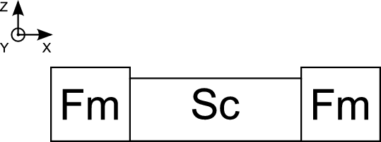
The originally by Datta and Das proposed spin transistor consists of one semiconductor layer and two ferromagnetic layers Figure 8.3.
To calculate the transport properties of a ballistic spin field-effect transistor a model similar to [15] and [54] is considered. The Hamiltonian in the ferromagnetic regions has the following form in the one-band effective mass approximation [47, 54, 53, 71]
 | (8.11) |
 | (8.12) |
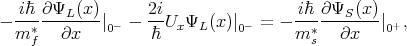
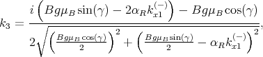
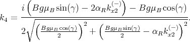
where mf* is the effective mass in the contacts, h 0 = 2PEF ∕(P2 + 1) is the exchange splitting energy with P defined as the spin polarization in the ferromagnetic regions, EF is the Fermi energy, and σz is the Pauli matrix; \B1 in (8.12) stands for the parallel and anti-parallel configuration of the contact magnetization. For the semiconductor channel region the Hamiltonian reads [15, 54]
 | (8.13) |
where ms* is the subband effective mass, δE c is the band mismatch between the ferromagnetic and the semiconductor region, αR is the strength of the spin-orbit interaction, g is the Land\B4e factor, μB is the Bohr magneton, B is the magnetic field, and σ* ≡ σ xcosγ + σysinγ with γ defined as the angle between the magnetic field and the transport direction.
To calculate the dependence of the transport properties on the spin-orbit interaction the electron eigenfunctions in the various regions are needed. For the ferromagnetic regions spin-up and spin-down eigenstates have the form (1, 0)† and (0, 1)†, respectively. The wave function in the left contact has the following form [15, 54]
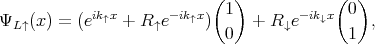 | (8.14) |
 | (8.15) |
where (8.14) represents the incoming spin-up electrons and (8.15) the incoming spin-down electrons, correspondingly,
k↑(↓) =  is the wave vector of the spin-up(spin-down) electron and R↑(↓) is the amplitude of the reflected
wave. To find eigenvectors to the corresponding vector k↑(↓) the Schr\A8odinger equation spin-up spinor for the right contact the
wave function is given by [15, 54]
is the wave vector of the spin-up(spin-down) electron and R↑(↓) is the amplitude of the reflected
wave. To find eigenvectors to the corresponding vector k↑(↓) the Schr\A8odinger equation spin-up spinor for the right contact the
wave function is given by [15, 54]
 | (8.16) |
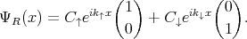
For the semiconductor region the wave function can be written as [15, 54]
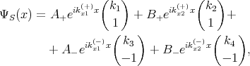 | (8.17) |
where kx1(x2)(+) and k
x1(x2)(-) are the wave vectors obtained by solving the equations  +δEc\B1
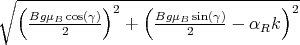 = E,
respectively.
= E,
respectively.
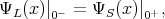
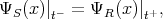
The usual boundary conditions are applied: the wave functions are continuous at the interfaces and that there is a step
discontinuity of the first derivative of the wave function over channel direction  due to an assumed delta-function-like
barrier at the interfaces between the ferromagnetic and the semiconductor region. Thus, boundary conditions are written
as [47]
due to an assumed delta-function-like
barrier at the interfaces between the ferromagnetic and the semiconductor region. Thus, boundary conditions are written
as [47]
 | (8.18) |
 | (8.19) |
 | (8.20) |
 | (8.21) |
The coefficients k1,k2,k3,k4 are calculated as [15, 54]
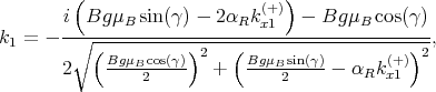 | (8.22) |
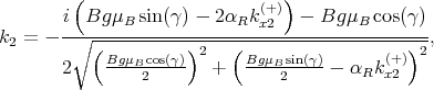 | (8.23) |
 | (8.24) |
 | (8.25) |
The reflection and transmission coefficients are determined by applying the boundary conditions at the ferromagnet/semiconductor interfaces.
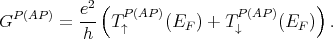
The current through the device is computed as [88, 89, 68]
![e ∫ ∞ [ P (AP ) P (AP ) ]
IP(AP)(V ) =-- T↑ (E ) + T↓ (E )
h{ δE }
1 1
-----E-EF-- -----E-EF+eV- dE,
1 + e kBT 1 + e kBT](disser271x.png) | (8.26) |
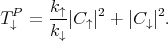
where kB is the Boltzmann constant, T is the temperature, and V is the voltage. The spin-up (T↑P ) and spin-down (T↓P ) transmission probabilities for the parallel configuration of the contact magnetization are defined as
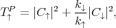 | (8.27) |
 | (8.28) |
For the anti-parallel configuration of the contact magnetization the transmission probabilities are given by
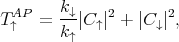 | (8.29) |
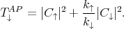 | (8.30) |
The conductance is defined as
 | (8.31) |
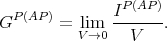
In the limit of low temperature the conductance must coincide with the one obtained from the Landauer-B\A8uttiker formula [68, 13]
 | (8.32) |
Finally, the tunneling magnetoresistance (TMR) is defined as [15, 54]
 | (8.33) |
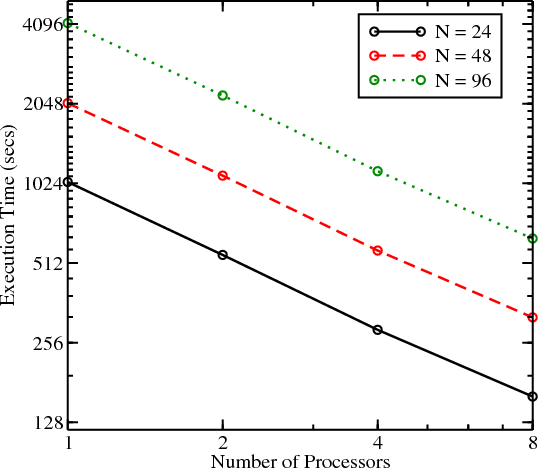
The dependence of the conductance through the silicon SpinFET on the physical parameters was investigated. In order to calculate the conductance one first has to determine the wave vectors, then compose the system of equations corresponding to the boundary conditions, and finally solve the obtained system of linear equations to gain the transmission coefficients for the spin-up and spin-down electrons. These calculations must be performed for the parallel and the anti-parallel configuration of the contact magnetization for each energy point of the half-infinite integrand (8.26). It follows from (8.32) that the integral evaluated numerically describes the conductance for a single point of the conduction band mismatch δEc, at a single value of temperature T. Thus to investigate the transport properties of the silicon SpinFET at various parameter values a huge amount of calculations must be carried out. To reduce the simulation time the code for the model must be heavily optimized and parallelized.
The usual techniques for parallelization are divided into two groups - parallelization in case of shared-memory and parallelization in case of distributed memory systems. The advantage of shared-memory parallelization is that it guarantees uniform access to the memory for each process. This means that the time spent for data manipulation in the memory is approximately the same for each process. The advantage of distributed calculations is that the number of processors used for the calculations is not limited to the number of processors on a single node.
In the simulations the code is parallelized with the OpenMP library. Because of the absence of the correlation between the conductances at different energy points the whole calculations are distributed between a large number of computing threads. Thus the time spent for the calculations is reduced proportionally to the number of parallel threads. Although threads perform calculations in parallel, the time spent by each thread to fulfill the tasks is not the same. Therefore one has to take proper care of a uniform distribution of the computational load between the threads. This problem is crucial for obtaining the maximum possible speed-up. Since OpenMP provides a possibility to control the amount of calculations for each thread in the run-time mode, the problem of the uniform distribution of the computational load is solved by standard tools.
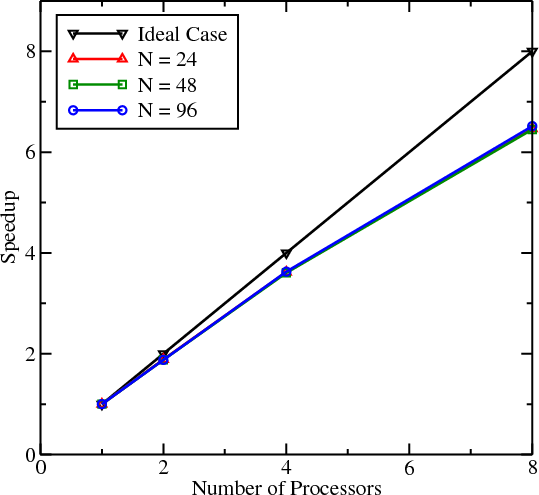
The performance of the code has been improved by utilizing the OpenMP approach. The results of using the parallel implementation are presented in Table 8.1. The actual speedup of the code is very close to the ideal (linear) speedup, in which the increase of the number of processors (cores) by two leads to the decrease in the computing time by two. This excellent improvement is possible due to the already mentioned fact that there is no correlation between the calculations of the conductances.
Calculations in the presence of temperature require high accuracy. Therefore, the adaptive methods from the GNU Scientific Library [2] have been used for the numerical integration.
| Number of Processors | N=24 | N=48 | N=96 |
| 1 | 1036 | 2057 | 4129 |
| 2 | 549 | 1094 | 2198 |
| 4 | 286 | 570 | 1138 |
| 8 | 160 | 318 | 633 |
Two types of material for the semiconductor region are used: InAs, which is characterized by a strong value of the spin-orbit interaction, and silicon, which is characterized by a moderate value of the spin-orbit interaction.
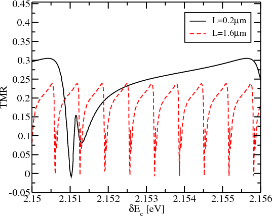
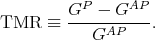
All calculations for the InAs semiconductor channel assume that the dominant mechanism of the spin-orbit coupling due to the geometry-induced inversion symmetry breaking (Rashba type). Common simulation parameters are as follows: the effective mass for the ferromagnetic region mf* = m 0 and for the semiconductor region ms*=0.036m 0, where m0 is the electron rest mass. Figure 8.6 shows the dependence of the TMR on the value of the band mismatch δEc between the ferromagnetic source contact and the semiconductor channel. The TMR oscillates between positive and negative values. As the length of the semiconductor channel decreases, the period of the oscillations increases roughly proportionally to the inverse length of the semiconductor channel.
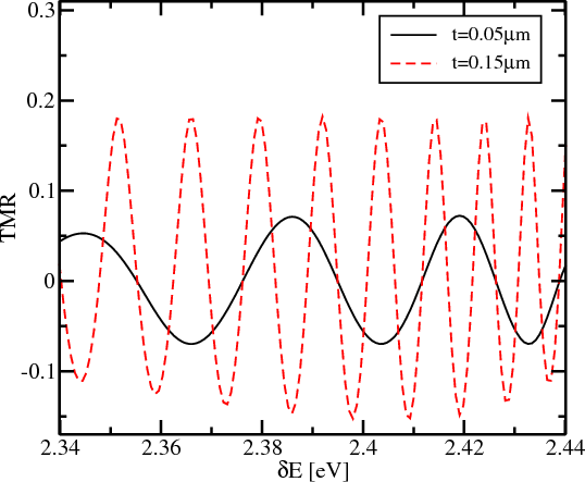
The temperature exerts a significant influence on the device characteristics as shown in Figure 8.7. For a channel length t=0.05μm the oscillatory amplitude of the TMR decreases for T=77K and completely vanishes for T=180K. The reason for the oscillatory behavior to disappear at T=180K is a relatively short period of the conductance oscillations (and correspondingly TMR oscillation shown in Figure 8.6) with respect to δEc. Thus, one can expect that for the shorter channel the amplitude of oscillations is sufficient to modulate the current in the SpinFET at higher temperatures.
To facilitate the injection of the spin-polarized current into the channel, following [15] and [54], delta-function barriers of
strength z = 2mf*U∕h2k
F , where kF =  , at the interfaces between the contacts and the channel are introduced.
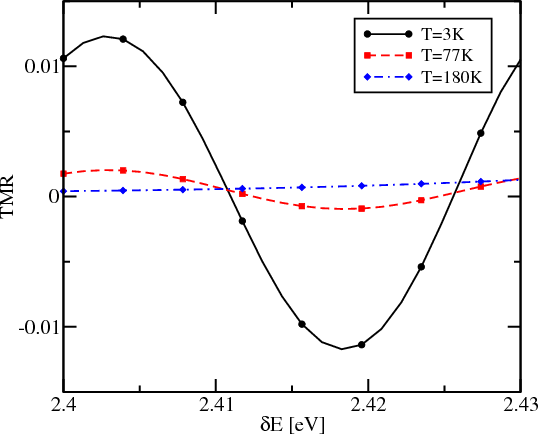
The current dependence on the value of the drain-source voltage is shown in Figure 8.8. A clear S-like shape of the curves is
observed at T=10K. This is a manifestation of the conductance oscillations as a function of δEc, which have
a large amplitude due to the presence of the delta-function barriers at the interfaces between the contact
and the channel (z=3). A large amplitude of the conductance oscillations guarantees the different slopes of
the I-V curves corresponding to different δEc. Although the S-like non-linearity is not well pronounced at
higher temperatures, the difference in the slopes at small voltages is not completely washed out, even at room
temperature.
, at the interfaces between the contacts and the channel are introduced.
The current dependence on the value of the drain-source voltage is shown in Figure 8.8. A clear S-like shape of the curves is
observed at T=10K. This is a manifestation of the conductance oscillations as a function of δEc, which have
a large amplitude due to the presence of the delta-function barriers at the interfaces between the contact
and the channel (z=3). A large amplitude of the conductance oscillations guarantees the different slopes of
the I-V curves corresponding to different δEc. Although the S-like non-linearity is not well pronounced at
higher temperatures, the difference in the slopes at small voltages is not completely washed out, even at room
temperature.
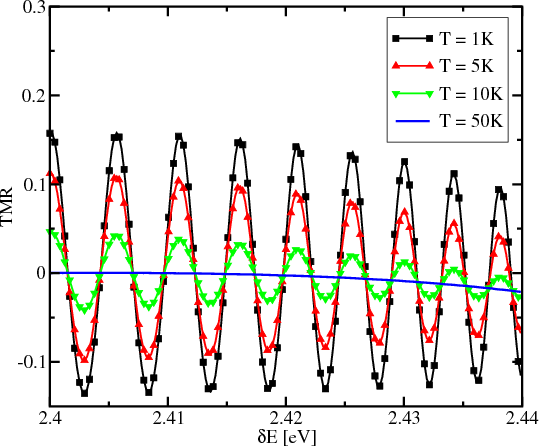
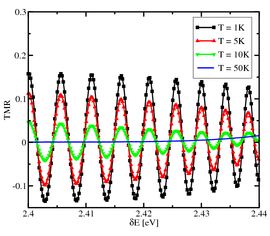
Figure 8.9 and Figure 8.10 show the dependence of the TMR on the band mismatch between the source/drain contacts and the semiconductor region, for several temperatures in absence of a magnetic field and under an applied field of 3T. At low temperatures the TMR oscillates around zero, and the strength of the magnetic field does not influence the oscillations much, which is in agreement with [54]. As the band mismatch increases, influence of the magnetic field becomes more significant. Also, one can see that increasing the temperature leads to a dramatic decrease in the amplitude of the TMR oscillations and reduces the ability to modulate the TMR by adjusting the band mismatch.
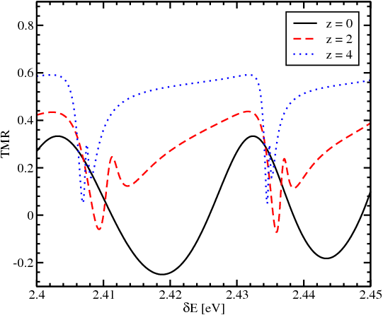
Another option to proceed to higher temperatures is to boost the value of the TMR by exploiting its dependence on αR. Figure 8.11 illustrates the corresponding change. As the barriers become stronger the quantization of the energy in the semiconductor channel becomes more pronounced. The energy quantization is responsible for the appearance of the sharp peaks on the TMR dependence on δEc clearly seen in Figure 8.11. An excellent feature following from Figure 8.11 is that the TMR value remains positive in a broad range of δEc. Most importantly, the sign and the values of the TMR depend on the strength of the spin-orbit interaction. It then follows that in the presence of the barriers between the contact and the channel the values of the TMR must depend on the strength of the spin-orbit interaction controlled by the gate voltage at elevated temperatures as well. Next this consideration [54, 15] is generalized to finite temperatures.
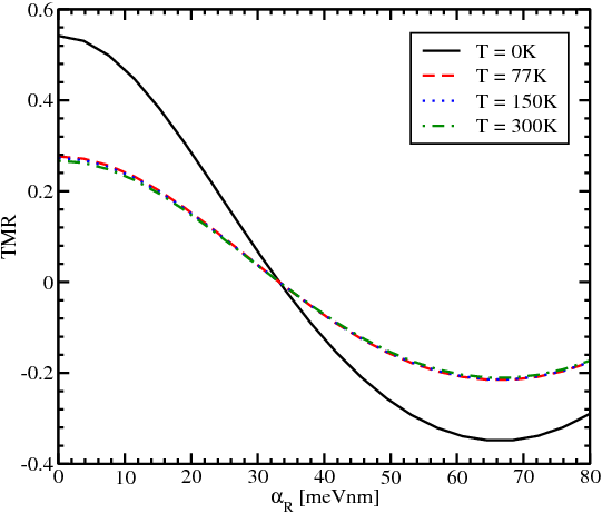
Figure 8.12 displays the TMR dependence on the strength of the spin-orbit interaction at different temperatures. The TMR modulation is preserved at elevated temperatures, thus opening a practical possibility to control the TMR by changing the value of αR even at room temperature.
Square silicon fins with [100] or [110] orientation, with (001) horizontal faces are considered. The parabolic band approximation for the band structure in silicon is not sufficient to accurately obtain the subband structure in thin and narrow silicon fins. The two-band k⋅p model proposed in [9] is employed, which has been shown to be accurate up to 0.5eV above the conduction band edge in silicon [112]. The resulting Schr\A8odinger differential equation, with the confinement potential appropriately added to the Hamiltonian [9], is discretized using the box integration method and solved for each value of the conserved momentum px along the current direction using efficient numerical algorithms available through the Vienna Schr\A8odinger-Poisson framework (VSP) [62].
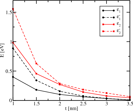
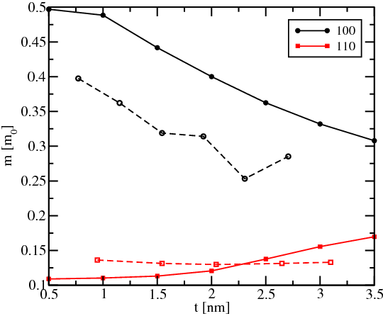
Figure 8.13 demonstrates the dependence of the subband minima as function of the fin thickness t for the lowest four subbands; the fin orientation is along the [110] direction. The dependence of the splitting between the unprimed subbands with decreasing t, which are perfectly degenerate in the effective mass approximation, is clearly seen. The splitting between valleys in a [100] fin is negligible [114]. In contrast to that, the dependence of the effective mass of the ground subband in [100] fins on t is more pronounced as compared to [110] fins. Results of density-functional calculations [114] confirm the mass dependences obtained from the k⋅p model (Figure 8.14).
With the values of the effective masses and subband offsets obtained, the conductance properties for the parallel and anti-parallel configurations of the contact magnetization is studied. The spin-orbit interaction is treated in the Dresselhaus form (8.9). The Hamiltonian in the channel for [100] oriented fins reads
 | (8.34) |
and
 | (8.35) |
for [110] oriented fins. Here mn* is the subband effective mass, δE n is the subband mismatch between the ferromagnetic region and the channel, and β is the strength of the spin-orbit interaction.
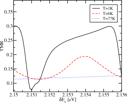
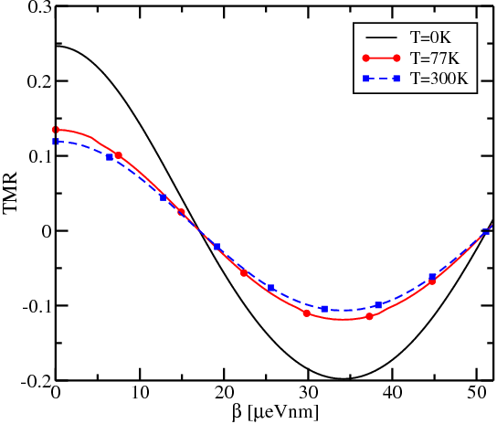
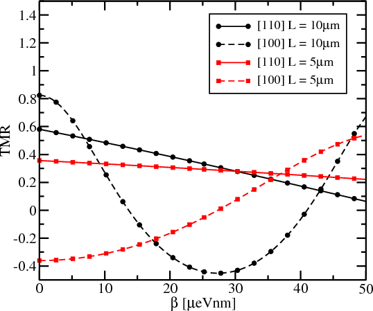
Figure 8.15 shows the dependence of the TMR for [100] and [110] oriented fins with t = 1.5nm on the value of the spin-orbit interaction. Fins with [100] orientation show a stronger dependence on β compared to [110] oriented fins. Thus [100] oriented fins are preferred for silicon SpinFETs. The reason of the stronger dependence is that the characteristic length on which the spin-orbit interaction produces the full spin precession is defined by the inverse of the wave vector kD = mn*β∕ℏ2. As shown in Figure 8.14, the effective mass value for the [110] oriented fins is smaller compared to the [100] oriented fins, hence for the same variation of kD in case of the [110] oriented fins a larger variation of β is required to achieve the same TMR value modulation.
Figure 8.16 shows the dependence of the oscillations of the TMR on the value of the conduction band mismatch δEc. The period of the oscillations is roughly inversely proportional to the length of the semiconductor channel as also shown in Figure 8.6. The presence of the delta-function barriers at the interfaces between the contact and the channel exerts a significant influence on the oscillation shape. For higher and thicker barriers, the TMR, although being a periodic function of the conductance band mismatch, stops oscillating around zero and becomes positive (or negative) in a broad range of the conduction band mismatch. This sign definitiveness leads to the complete absence of the oscillations of the TMR at T=77K as shown in Figure 8.17. It is important that, although reduced, the TMR is not zero at 77K. Therefore, the TMR modulation as a function of the spin-orbit interaction strength is preserved even at high temperatures as shown in Figure 8.18. This opens the possibility to modulate the TMR by changing the value of β even at room temperature.