Next: 3.2 Lattice and Thermal
Up: 3.1 Sets of Partial
Previous: 3.1.5 The Insulator Equations
Subsections
3.1.6 Boundary Conditions
The basic semiconductor equations are posed in a bounded domain. At the
boundaries of this domain appropriate boundary conditions need to be specified
for the unknowns  ,
,  ,
,  ,
,  ,
,  , and
, and
 .
.
In order to separate the simulated device from neighboring devices, artificial
boundaries must be specified which are not boundaries in a physical sense.
The Neumann boundary condition guarantees that the simulation domain
is self-contained and there are no fluxes across the boundary.
| |
|
 |
(3.20) |
| |
|
 |
(3.21) |
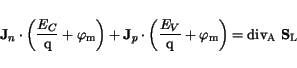
Here,  denotes an outward oriented vector normal to the boundary.
(3.20) and (3.21) give the
boundary conditions at the artificial boundaries for semiconductor and
insulator segments, respectively.
denotes an outward oriented vector normal to the boundary.
(3.20) and (3.21) give the
boundary conditions at the artificial boundaries for semiconductor and
insulator segments, respectively.
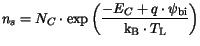
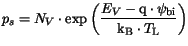
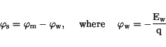
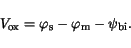
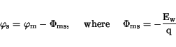
At Ohmic contacts simple Dirichlet boundary conditions apply. The
contact potential
 , the carrier contact concentrations
  and
and  , and in
the HD simulation case, the contact carrier temperatures and are
fixed. The metal quasi-Fermi level (which is specified by the
contact voltage
, and in
the HD simulation case, the contact carrier temperatures and are
fixed. The metal quasi-Fermi level (which is specified by the
contact voltage
 ) is equal to the semiconductor quasi-Fermi
level. The contact potential at the semiconductor boundary reads
) is equal to the semiconductor quasi-Fermi
level. The contact potential at the semiconductor boundary reads
 |
(3.22) |
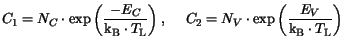
The built-in potential
 is calculated after [76]
Here,  is the net concentration of dopants and other charged defects at the
contact boundary. The auxiliary variables
is the net concentration of dopants and other charged defects at the
contact boundary. The auxiliary variables  and
and  are defined by
| |
|
 |
(3.24) |
The carrier concentrations in the semiconductor are pinned to the equilibrium carrier concentrations at the contact. They are expressed as
| |
|
 |
(3.25) |
| |
|
 |
(3.26) |
The carrier temperatures and are set equal to the lattice temperature
.
| |
|
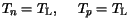 |
(3.27) |
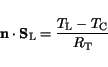
In the case of a thermal contact the lattice temperature
is calculated
using a specified contact temperature
 and thermal resistance
 .
The thermal heat flow density
.
The thermal heat flow density
 at the contact boundary reads:
 |
(3.28) |
In case no thermal resistance is specified an isothermal boundary condition is
assumed and the lattice temperature
is set equal to the contact
temperature
.
 |
(3.29) |
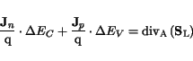
In the case of DD simulation with self-heating an additional thermal energy is
accounted for. This thermal energy is produced when the carriers have to
surmount the potential difference between the conduction or valence band and
the metal quasi-Fermi level. The energy equation reads:
 |
(3.30) |
The expression
 denotes the surface
divergence of the thermal heat flux at the considered boundary. In the case of
HD simulation with self-heating the thermal heat flow across the boundary is
accounted for self-consistently.
denotes the surface
divergence of the thermal heat flux at the considered boundary. In the case of
HD simulation with self-heating the thermal heat flow across the boundary is
accounted for self-consistently.
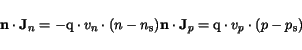
At the Schottky contact mixed boundary conditions apply. The contact potential
, the carrier contact concentrations and , and in the HD
simulation case, the contact carrier temperatures and are
fixed. The semiconductor contact potential is the difference of the metal
quasi-Fermi level (which is specified by the contact voltage
) and the metal workfunction difference
potential
 .
.
 |
(3.31) |
The difference between the conduction band energy  and the metal
workfunction energy gives the workfunction difference energy
and the metal
workfunction energy gives the workfunction difference energy
 which is
the so-called barrier height of the Schottky contact. The applied boundary
conditions are
which is
the so-called barrier height of the Schottky contact. The applied boundary
conditions are
 |
(3.32) |
Here  and
and  are the thermionic recombination velocities. The carrier
concentrations are expressed as
are the thermionic recombination velocities. The carrier
concentrations are expressed as
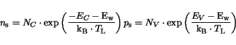 |
(3.33) |
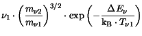
The default values for and are set to 0 (see Table 3.1) which
suppresses current flow through the Schottky contact
(
 ).
).
Table 3.1:
Parameter values for Schottky contact model
| Material |
[eV] |
[m/s] |
[m/s] |
| n-Si/Au |
-0.55 |
0.0 |
0.0 |
| p-Si/Au |
0.55 |
0.0 |
0.0 |
| others |
0.0 |
0.0 |
0.0 |
|
The Schottky contact boundary conditions for the carrier temperatures and
and the lattice temperature
are similar to the ones which apply for
the Ohmic contact, i.e. (3.27) and (3.28),
or respectively (3.29).
3.1.6.2.3 Polysilicon Contact
In MINIMOS-NT the polysilicon contact model after [77] is implemented.
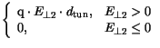
The dielectric flux  through the oxide reads
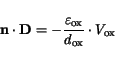 |
(3.34) |
where
 is the voltage drop over the thin oxide layer which is
introduced between polysilicon and silicon,
is the voltage drop over the thin oxide layer which is
introduced between polysilicon and silicon,
 and
and
 denote
respectively the permittivity and thickness of this layer. The electron and
hole current densities across the contact interface read
denote
respectively the permittivity and thickness of this layer. The electron and
hole current densities across the contact interface read
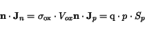 |
(3.35) |
where
 is the oxide conductivity, is the hole
concentration in the semiconductor, and
is the oxide conductivity, is the hole
concentration in the semiconductor, and  is the hole surface
recombination velocity.
depends on the quasi-Fermi
level in the metal (which is specified by the contact voltage
), the
potential in the semiconductor
, and the built-in potential
.
is the hole surface
recombination velocity.
depends on the quasi-Fermi
level in the metal (which is specified by the contact voltage
), the
potential in the semiconductor
, and the built-in potential
.
 |
(3.36) |
The polysilicon contact boundary conditions for the carrier temperatures and
and the lattice temperature
are similar to the ones which apply for
the Ohmic contact, i.e. (3.27) and (3.28),
or respectively (3.29).
In the case of insulator-metal boundaries a model similar to the Schottky
contact model is used to calculate the insulator contact potential. The
semiconductor contact potential is the difference of the metal
quasi-Fermi level (which is specified by the contact voltage
) and the metal workfunction difference potential
 .
.
 |
(3.37) |
Again,
is the workfunction difference energy. The lattice temperature
is set equal to the contact temperature (3.29).
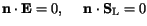
In the absence of surface charges at the semiconductor-insulator interface the
normal component of the dielectric displacement is continuous, and so is the potential.
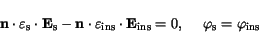 |
(3.38) |
In the presence of surface charges along the interface the dielectric
displacement obeys the law of Gauß
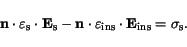 |
(3.39) |
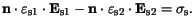
At the semiconductor-insulator interface the carrier current densities (or
driving forces) and the carrier heat fluxes normal to the interface vanish.
| |
|
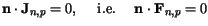 |
(3.40) |
| |
|
 |
(3.41) |
The lattice temperature at the interface is continuous.
Similarly to the semiconductor-insulator interface (3.38) or
(3.39) apply depending on the presence of surface charges.
The lattice temperature must be continuous.
3.1.6.6 Semiconductor-Semiconductor Interface
The calculation of the electrostatic potential at interfaces between two
semiconductor segments is similar to the one at semiconductor-insulator
interfaces.
| |
|
 |
(3.42) |
| |
|
 |
(3.43) |
Here
 is the interface charge density which can be zero or non-zero.
The subscripts are used to distinguish between the two semiconductor segments
on both sides of the interface.
is the interface charge density which can be zero or non-zero.
The subscripts are used to distinguish between the two semiconductor segments
on both sides of the interface.
To calculate the carrier concentrations and the carrier temperatures at the
interface of two semiconductor segments three different models are considered
These are a model with continuous quasi-Fermi level across the
interface (CQFL), a thermionic emission model (TE), and a
thermionic field emission model (TFE). The derivation of these
models is given in [78]. Each model can be specified separately for
electrons and holes for each semiconductor-semiconductor interface.
In the following  denotes the current density,
  the energy flux density,
and
the energy flux density,
and
 the difference in the conduction or valence band edges,
respectively. The carrier concentration is denoted by
the difference in the conduction or valence band edges,
respectively. The carrier concentration is denoted by  . The subscripts
denote the semiconductor segment and the carrier type.
. The subscripts
denote the semiconductor segment and the carrier type.
 |
 |
 |
(3.46) |
|
|
 |
(3.47) |
 |
|
 |
(3.48) |
|
|
 |
(3.49) |
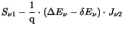
with the thermionic emission velocity (3.50) and the
barrier height lowering (3.51).
The barrier height lowering depends on the electric field orthogonal to the
interface  and the effective tunneling length
 . For
. For
 the TFE model reduces to the TE model.
By using the CQFL model a Dirichlet interface condition is applied.
The carrier concentrations are directly determined in a way that the
quasi-Fermi level across the interface remains continuous. The model
is suitable for use at homojunctions. However, it is erroneous to assume
continuous quasi-Fermi levels at abrupt heterojunctions. Also the
bandgap alignment of the adjustent semiconductors is ignored when such
continuous condition is enforced. Therefore, models using a
Neumann interface condition, like the TFE model or the TE model,
which determine the current flux across the interface, must be used.
Modeling the electron and hole current as well as the energy flux across
heterointerfaces is a complex task. Several models for different types of
interfaces have been proposed [79,80,81,82]. The TE model is
commonly used to model the current across heterojunctions of compound
semiconductors. The TFE model extends the TE model by accounting for tunneling
effects through the heterojunction barrier by introducing a field dependent
barrier height lowering. In [83] a method for unified treatment of
interface models was presented. It allows a change of the interface condition
from Neumann to Dirichlet type in the limit case of very
strong barrier reduction due to tunneling.
The lattice temperature is assumed to be continuous across
semiconductor-semiconductor interfaces. In the case of DD simulation with
self-heating an additional thermal energy is accounted for at heterojunction
interfaces. This thermal energy is produced when the carriers have to surmount
the energy difference in the conduction and valence bands,  and
and
 , respectively. The energy equation reads:
 |
(3.52) |
The expression
denotes the surface
divergence of the thermal heat flux at the considered boundary. In the case of
HD simulation with self-heating the thermal heat flow across the boundary is
accounted for self-consistently.
Next: 3.2 Lattice and Thermal
Up: 3.1 Sets of Partial
Previous: 3.1.5 The Insulator Equations
Vassil Palankovski
2001-02-28