


Next: 3.4.3 Surface scattering
Up: 3.4 Carrier Mobility
Previous: 3.4.1 Lattice Mobility
Subsections
3.4.2 Ionized Impurity Scattering
In semiconductor devices mobility reduction due to ionized impurity scattering
is a dominant effect. The influence of lattice and impurity scattering must
be combined to obtain an effective mobility
 . In MINIMOS-NT the
following models are available.
. In MINIMOS-NT the
following models are available.
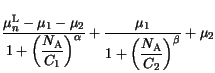
To account for mobility reduction due to ionized impurity scattering, the
formula of Caughey and Thomas [163] is used in conjunction with temperature
dependent coefficients.  denotes the concentration of ionized
impurities. The model is well applicable for Si.
denotes the concentration of ionized
impurities. The model is well applicable for Si.
 |
 |
 |
(3.97) |
 |
|
 |
(3.98) |
 |
|
 |
(3.99) |
 |
|
 |
(3.100) |
Simpler expressions are applied to other basic materials. By setting
 and
and
 ,
(3.98) and (3.100), respectively,
reduce to
,
(3.98) and (3.100), respectively,
reduce to
The model parameter values are
summarized in Table 3.22.
Table 3.22:
Parameter values for the impurity mobility
| Material |
 |
 [cm [cm /Vs] /Vs] |
 |
 |
 [cm [cm ] ] |
 |
 |
 |
| Si |
n |
80 |
-0.45 |
-0.15 |
1.12e17 |
3.2 |
0.72 |
0.065 |
| |
p |
45 |
-0.45 |
-0.15 |
2.23e17 |
3.2 |
0.72 |
0.065 |
| Ge |
n |
850 |
|
|
2.6e17 |
|
0.56 |
0.0 |
| |
p |
300 |
|
|
1.0e17 |
|
1.0 |
0.0 |
| GaAs |
n |
800 |
-0.9 |
-0.9 |
1.0e17 |
6.2 |
0.5 |
0.0 |
| |
p |
40 |
|
|
1.0e17 |
0.5 |
1.0 |
0.0 |
| AlAs |
n |
10 |
|
|
1.0e17 |
|
0.5 |
0.0 |
| |
p |
5 |
|
|
2.9e17 |
0.5 |
1.0 |
0.0 |
| InAs |
n |
11700 |
-0.33 |
-0.33 |
4.4e16 |
3.6 |
0.5 |
0.0 |
| |
p |
48 |
|
|
2.55e17 |
0.5 |
1.0 |
0.0 |
| InP |
n |
1520 |
2.0 |
2.0 |
6.4e16 |
3.7 |
0.5 |
0.0 |
| |
p |
24 |
1.2 |
1.2 |
2.5e17 |
0.47 |
1.0 |
0.0 |
| GaP |
n |
76 |
-1.07 |
-1.07 |
2.85e17 |
1.8 |
0.5 |
0.0 |
| |
p |
27 |
|
|
2.33e17 |
|
1.0 |
0.0 |
|
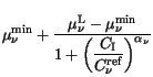
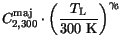
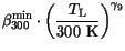
The results delivered by the model for the hole
mobility as a function of the doping concentration for various III-V group
binary semiconductors compared to measured data are shown in Fig. 3.33.
Figure 3.33:
Hole mobility vs. doping concentration at 300 K: Comparison
between the model and experimental data
|
|
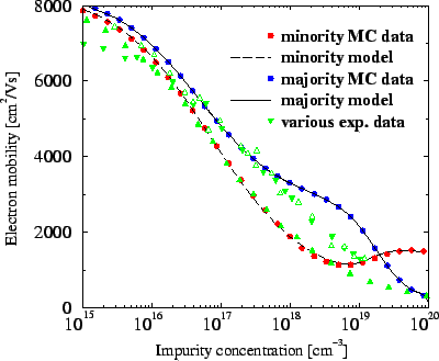
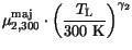
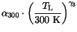
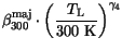
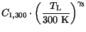
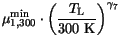
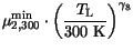
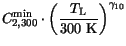
3.4.2.2 Model for Majority and Minority Electrons
Though numerous theoretical and experimental papers [164,165,166]
on electron mobility in semiconductors have been published there are still some
issues under discussion, particularly in the very high doping regime. The
difference between majority and minority electron mobility is a well-known
phenomenon caused by effects such as degeneracy and the different screening
behavior of electrons and holes in semiconductors. However, the mobility models
usually employed in device modeling do not reflect these facts.
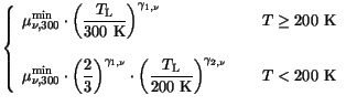
One of the basic assumptions in the models for ionized-impurity scattering is
that the charge of an impurity center is treated as a point charge. In the
approach from [140] it was shown that considering the spatial extent of
the charge density one can explain various doping effects due to the chemical
nature of the dopant at high doping concentrations. In [140]
Monte-Carlo (MC) simulation results for the low-field mobility in silicon,
covering arbitrary finite concentrations, temperatures and dopants are
presented (see Fig. 3.34 and Fig. 3.35).
Figure 3.34:
Majority mobility in P-, As- and Sb-doped silicon at 300 K:
Comparison between MC simulation data and experimental data
|
|
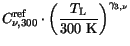
Figure 3.35:
Minority mobility in B-doped silicon as a function of concentration:
MC simulation data at different temperatures
|
|
The minority mobility at doping levels above  cm
exceeds the majority mobility more than three times at 300 K. The
difference gets even stronger at low temperatures (up to sixteen times).
cm
exceeds the majority mobility more than three times at 300 K. The
difference gets even stronger at low temperatures (up to sixteen times).
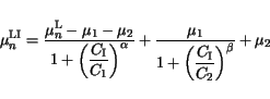
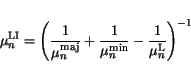
A model which distinguishes between the majority and minority electrons in
 , as well as between dopant species is described in [167,168,66].
Although initially proposed for the majority electron mobility in Si
, as well as between dopant species is described in [167,168,66].
Although initially proposed for the majority electron mobility in Si
 |
(3.103) |
offers enough flexibility to model also the minority electron mobility in Si
(see Fig. 3.36). In general, it can be applied also for any other material of
interest (Fig. 3.37, Fig. 3.38). (3.103) is similar to
(3.97), a function with two extreme values (
 as a
maximum and
as a
maximum and  as a minimum mobility). (3.103) is a mathematical
function which can deliver a second maximum or minimum at very high impurity
concentrations depending on the sign of . Thus, it allows both majority
and minority carrier mobilities to be properly modeled.
as a minimum mobility). (3.103) is a mathematical
function which can deliver a second maximum or minimum at very high impurity
concentrations depending on the sign of . Thus, it allows both majority
and minority carrier mobilities to be properly modeled.
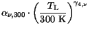
Figure 3.36:
Comparison of the analytical model and MC data for electron
mobility in Si at 300 K
|
|
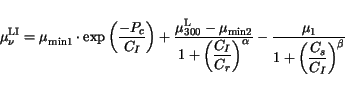
Figure 3.37:
Comparison of the analytical model and MC data for electron
mobility in InP at 300 K
|
|
Figure 3.38:
Comparison of the analytical model and MC data for electron
mobility in GaAs at 300 K
|
|
In [169] an automated parameter extraction using an optimizer
[170] for the mobility models was presented. Most of the
existing experimental data on the low-field mobility together with accurate MC
simulations for Si [140] and for III-V semiconductor compounds
[128,171,172] are used as input.
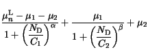
The temperature dependence of the lattice mobility
 preserves the
expression (3.96). The majority electron mobility
preserves the
expression (3.96). The majority electron mobility
 is modeled as a function of the donor concentration
  and the lattice temperature. The temperature dependence of the parameters
,
and the lattice temperature. The temperature dependence of the parameters
,  ,
,  ,
,  ,
,  , and
, and  is modeled by simple
power laws.
is modeled by simple
power laws.
 |
|
 |
(3.104) |
 |
|
 |
(3.105) |
 |
|
 |
(3.106) |
 |
|
 |
(3.107) |
 |
|
 |
(3.108) |
 |
|
 |
(3.109) |
 |
|
 |
(3.110) |
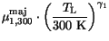
The minority electron mobility
 is modeled as a function of the
acceptor concentration
is modeled as a function of the
acceptor concentration  and the lattice temperature. The parameters
and preserve the values from (3.108) and
(3.110), respectively. The new parameters , , ,
and , used in the calculation of
, again follow simple
power laws as a function of temperature.
and the lattice temperature. The parameters
and preserve the values from (3.108) and
(3.110), respectively. The new parameters , , ,
and , used in the calculation of
, again follow simple
power laws as a function of temperature.
 |
|
 |
(3.111) |
|
|
 |
(3.112) |
|
|
 |
(3.113) |
|
|
 |
(3.114) |
|
|
 |
(3.115) |
To account for a superposition of doping profiles a harmonic mean is used [168].
 |
(3.116) |
The model parameters used for Si in the range 70-500 K and for GaAs and InP at
300 K are summarized in Table 3.23.
Table 3.23:
Parameter values for
the majority/minority impurity mobility
| Parameter |
Si |
GaAs |
InP |
Unit |
 |
52 |
2590 |
1140 |
 |
 |
-0.18 |
- |
- |
|
 |
8 |
133 |
20 |
|
 |
-1.49 |
- |
- |
|
 |
-200 |
-750 |
-742 |
|
 |
-0.58 |
- |
- |
|
 |
230 |
1400 |
1920 |
|
 |
-1.02 |
- |
- |
|
 |
0.7 |
0.7 |
0.6 |
|
 |
0.02 |
- |
- |
|
 |
5.33 |
1.7 |
2.5 |
|
 |
-9.5 |
- |
- |
|
 |
2.0 |
2.8 |
3.2 |
|
 |
-1.2 |
- |
- |
|
 |
1.17e17 |
0.5e17 |
4e16 |
 |
 |
3.55 |
- |
- |
|
 |
5.8e20 |
1.8e19 |
1.6e19 |
|
 |
0.134 |
- |
- |
|
 |
1.0e19 |
1.4e19 |
1.6e19 |
|
 |
0.12 |
- |
- |
|
|
3.4.2.3 Masetti Mobility Model
The Masetti bulk mobility model [173] is a
default mobility model in several device simulators, e.g. [40,41].
It can be treated as a simple case of (3.97), only valid at 300 K.
 |
(3.117) |
It can be useful to compare some of the parameters from the majority mobility model at 300 K
to the default values of the Masetti model (without  ) as it is shown in
Table 3.24.
) as it is shown in
Table 3.24.
Table 3.24:
Comparison between model parameters for majority electrons
in Si at 300 K and the parameter values for the Masetti impurity mobility model
| Parameter |
Si |
Parameter |
Masetti |
Unit |
|
|
52 |
 |
-56.1 |
|
|
|
8 |
 |
68.5 |
|
 |
60 |
 |
68.5 |
|
|
1.17e17 |
 |
9.2e16 |
|
|
|
5.8e20 |
 |
3.4e20 |
|
|
0.7 |
|
0.711 |
|
|
5.33 |
 |
-1.98 |
|
|
Next: 3.4.3 Surface scattering
Up: 3.4 Carrier Mobility
Previous: 3.4.1 Lattice Mobility
Vassil Palankovski
2001-02-28
![\resizebox{\halflength}{!}{
\includegraphics[width=\halflength]{figs/newh.eps}}](img487.gif)
![\resizebox{\halflength}{!}{
\includegraphics[width=\halflength,height=9.5cm]{figs/mobPAsSb.eps}}](img488.gif)
![\resizebox{\halflength}{!}{
\includegraphics[width=\halflength]{figs/mobB2.eps}}](img489.gif)
![\resizebox{\halflength}{!}{
\includegraphics[width=\halflength]{figs/si.eps}}](img492.gif)
![\resizebox{\halflength}{!}{
\includegraphics[width=\halflength]{figs/Cinpex2.eps}}](img493.gif)
![\resizebox{\halflength}{!}{
\includegraphics[width=\halflength]{figs/Cgaasex.eps}}](img494.gif)