The result for the electron current density at V![]() = 1.5 V
(V
= 1.5 V
(V![]() ) is shown in Fig. 4.42. Note, the comparatively high electron
current portion of the base current. The simulation gives an explanation of the
experimentally observed decrease in the current gain at high bias. Comparisons
between the measured and simulated forward Gummel plot (Fig. 4.43) and current
gain (Fig. 4.44) show good agreement.
) is shown in Fig. 4.42. Note, the comparatively high electron
current portion of the base current. The simulation gives an explanation of the
experimentally observed decrease in the current gain at high bias. Comparisons
between the measured and simulated forward Gummel plot (Fig. 4.43) and current
gain (Fig. 4.44) show good agreement.
In the case of simulation of the output characteristics one meets severe
problems to achieve realistic results, especially in the case of power
devices. Therefore, self-heating (SH) effects have to be accounted for by
solving the lattice heat flow equation self-consistently with the energy
transport equations. An alternative Global SH model (GSH) has been offered in
[211]. The model calculates a spatially constant (global) lattice temperature
![]() in the device from the dissipated power as
in the device from the dissipated power as
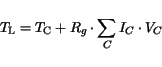 |
(4.5) |
In Fig. 4.45 the simulated output device characteristics compared to
measurements for base currents of 2, 4, 6, and 8 ![]() A are shown. The GSH
model with
A are shown. The GSH
model with ![]() = 800 K/W delivers the same results (within 2%) as the SH
model, but for 40% less CPU time. Both models deliver results in very good
agreement with the measured output device characteristics. In contrast to that,
simulation without including of SH effects cannot reproduce the experimental
data, especially at high power levels. Similar and even stronger observation
were already done in the case of GaAs power HBTs (see Section 4.2.2).
= 800 K/W delivers the same results (within 2%) as the SH
model, but for 40% less CPU time. Both models deliver results in very good
agreement with the measured output device characteristics. In contrast to that,
simulation without including of SH effects cannot reproduce the experimental
data, especially at high power levels. Similar and even stronger observation
were already done in the case of GaAs power HBTs (see Section 4.2.2).
![\resizebox{\halflength}{!}{
\includegraphics[width=\halflength]{figs/Camsout.eps}}](img803.gif)
|
![\resizebox{\halflength}{!}{
\includegraphics[width=\halflength]{figs/CfgpPoly.eps}}](img798.gif)
![\resizebox{\halflength}{!}{
\includegraphics[width=\halflength]{figs/CgainPoly.eps}}](img799.gif)