


From the experimental point of view Rutherford backscattering and channeling
analysis can be used to monitor the realignment process. A particle beam
(He) is injected at a predefined crystal orientation and the backscattered
spectra are detected. It allows some statements about the crystal
composition of the investigated material. Figure 3.2-5 shows the
RBS-C spectra for random as well as for aligned polysilicon material. Some
additional information about the realignment can be obtained from the slopes
of the low-energy edge. It can be seen that the realignment process takes
place by a planar motion of the alignment front towards the surface. After
90s the complete layer is realigned with a RBS-C minimum yield of ![]() which indicates a non-perfect crystal (
which indicates a non-perfect crystal ( ![]() yield equals perfect
crystal). With this RBS measurements it is now possible to trace the
realignment process in terms of crystal quality and realignment time.
yield equals perfect
crystal). With this RBS measurements it is now possible to trace the
realignment process in terms of crystal quality and realignment time.
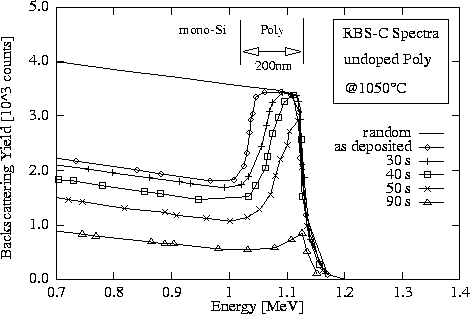
Figure 3.2-5: Rutherford backscattering spectra
for random (solid line) and aligned polysilicon along the ;SPMlt;100;SPMgt; direction
for a 200nm thick undoped polysilicon layer annealed at ![]() . The final yield is related to the crystal quality and the slope of the
spectra to the realignment front .
. The final yield is related to the crystal quality and the slope of the
spectra to the realignment front .
Epitaxial alignment requires silicon seed crystals to jump over the poly-/monosilicon interface, which can only happen when the oxide has broken up or the temperature is high enough. Despite of being an intensive area of research, no clear explanation has been proposed for the mechanism by which the interface oxide breaks up. Early models suggested that break-up starts at random pinholes sites, proceeded by oxygen surface diffusion to enlarge the sites and form circular beads [Adj91] . It is now clear from theoretical and transmission electron microscopy (TEM) analysis that the oxide starts to break up at grain boundaries which terminate at the interface [Spi93] [Sro86] . Figure 3.2-6a illustrates the initial conditions before the native oxide breaks up. Due to the fast diffusion pathes given by grain boundaries it is possible for the interface oxygen to diffuse towards the surface, and hence the interfacial oxide layer is thinned at this position until a slit has been formed (see Fig. 3.2-6b). It is also possible that the driving force for the break-up arises from thermal stress. Stress is relieved by contraction of the oxide layer and thus the surface area energy of the native oxide layer is increased. This is a necessity for forming slits due to the increasing surface. This could be the reason for additional slits generated at interface positions where no grain boundary terminates.
Once the slits are established, the next stage is the coalescence of the oxide fragments into oxide spheres. This transition is accompanied by grain boundary motion which results in the formation of triangular regions of epitaxially realigned silicon (see Fig. 3.2-6c). The surface area of these newly generated grain boundaries will be larger than the area of the eliminated ones, thus the grain boundaries are pinned onto the oxide fragments until the transition into oxide spheres has been completed. It should be noted that stress-generated slits have no fast diffusion pathes for gaining the realignment process. They are able the coalesce because of the lateral extend of the realignment process.
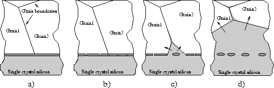
Figure: Schematic
interpretation of the early stages of epitaxial realignment of polysilicon
films. The realignment starts at native oxide slits and moves along the
grain boundaries towards the surface. The remaining native oxide layer
agglomerates into spherical beads; a) initial setup b) oxide break-up c)
starting of realignment d) full realigned interface with oxide beads.
The proceeding alignment process depends on the initial microstructure
and the dopant concentrations dispersed in the polysilicon layer. The key
role in the further alignment plays the dopant type and the initial grain
size. It can be seen from TEM images that for doped boron polysilicon with
relatively small grains (compared to the film thickness) the realignment
front moves towards the surface in a more or less regular front. At the
grain boundary sites the realignment extends deeper into the layer, like
demonstrated in Figure 3.2-6d. Once the partial realignment has
reached the surface, lateral epitaxial growth starts from the grain
boundaries into the grain bulks. RBS spectra show whether the growth occurs
laterally or vertically. In the case of continuous vertical realignment the
spectra peaks are decreasing and the width of the spectra slope, which can
be seen as the unaffected polysilicon random material, moves towards the
surface (see Fig. 3.2-5). When polysilicon deposited at
temperatures above ![]() (which leads to grain sizes in the order of
the film thickness) is realigned, the growth front reaches quickly the
surface and the main epitaxial growth is obtained by lateral growth. The
peak in the corresponding RBS spectra shows a constant width, which implies
a not well-arranged alignment front (see Fig. 3.2-7).
Realignment rate activation energies extracted from literature are in the
order of the activation energies for dopant diffusion which seems to be the
limiting factor for the realignment process [Spi93]
.
(which leads to grain sizes in the order of
the film thickness) is realigned, the growth front reaches quickly the
surface and the main epitaxial growth is obtained by lateral growth. The
peak in the corresponding RBS spectra shows a constant width, which implies
a not well-arranged alignment front (see Fig. 3.2-7).
Realignment rate activation energies extracted from literature are in the
order of the activation energies for dopant diffusion which seems to be the
limiting factor for the realignment process [Spi93]
.
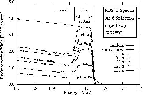
Figure 3.2-7: Rutherford
backscattering spectra for random (solid line) and aligned polysilicon along
the ;SPMlt;100;SPMgt; direction for a 200nm thick polysilicon layer annealed at
![]() . The remaining width of the slope refers to lateral epitaxial
growth of the layer .
. The remaining width of the slope refers to lateral epitaxial
growth of the layer .
However, in actual device fabrication the shared interface area of the
polysilicon film with the crystalline silicon substrate is limited. If the
film dimensions are reduced to the order of the polysilicon grain size, size
effects are arising for the epitaxial realignment. The thickness of the
polysilicon layer influences the onset of lateral regrowth, and the length of
the interface controls the uniformity and the total realigned fraction of
the layer. In ![]() polysilicon emitter technology a retardation of
the realignment rate was observed in the bended regions of the layer. This
effect slows down the realignment kinetics and increases the thermal budget
needed to complete the realignment of films deposited on narrow strips.
polysilicon emitter technology a retardation of
the realignment rate was observed in the bended regions of the layer. This
effect slows down the realignment kinetics and increases the thermal budget
needed to complete the realignment of films deposited on narrow strips.
To reduce process sensitivity and emitter resistance in high performance bipolar technology a short high temperature emitter drive-in is favored. Whilst a furnace annealing process leads to a partially realigned layer with uncontrolled properties of the interface, RTA processing can provide better alignment conditions and due to the lower thermal budget less dopant diffusion.
Simulation of RTA outdiffusion processes from polysilicon is important for bipolar and BiCMOS engineering. The occurrence of realignment has to be incorporated into a diffusion model. The original orientation of the grains, obtained from a deposition simulation, must be changed to the orientation of the underlying substrate seed crystal. The interface conditions change significantly after break-up which must be traced by the interface model. Within this work we present an interface model which consists of three stages. During the first stage, lasting as long as the native oxide is intact, we apply a segregation model for the dopant transport across the interface. Once the interface has broken up, we switch to a conduction model with a time dependent contact area for the transition of the oxide from fragments into spheres. An interface conduction model with a fixed area deduced from the remaining slit area is used when the interface is fully aligned. Details on the applied interface models are given in Section 4.4.
Summarizing, simulation of diffusion inside polysilicon layers requires the coupled solution of the diffusion equations for the grain boundary and the grain interior dopant species including the grain growth relation. The dopant transport across material borders has to be captured by segregation or conduction kinetics. A full description including the physical parameters for a polysilicon diffusion model is given in Section 4.3.5.