


One of the main applications for polysilicon layers is to serve as outdiffusion source. Polysilicon layers are deposited on top of the substrate and excessively high doped. During the subsequent furnace (FA) or RTA annealing step dopants diffuse from the polysilicon into the underlying substrate. The amount of outdiffused dopants depends on the applied thermal budget and the structure of the interface. The dopant transport during this anneal in the polysilicon as well as across the interface is a very complex mechanism being still an area of interest for many researchers [Han93] [Mat93b] [Jon90].
It is known from experiments, that polysilicon shows extraordinary high diffusivity for dopants. This fact allows the dopants to diffuse even long distances within the polysilicon material in reasonable short time periods.
Dopant transport within polysilicon involves four major mechanism:
To gain insight into the dopant/grain boundary system and the according diffusion mechanisms, we take a closer look onto the crystal structure of a grain bulk/grain boundary network. Figure 3.2-4 gives the subtle tetrahedral bonding network for two polysilicon grains separated by a grain boundary. It can be seen that the number of bonds crossing from one grain into the neighboring grain is reduced at the interface, so that the fracture of the crystal along the interface causes a corresponding low density of dangling bonds. Therefore, we suggest that this boundary area may be a preferred low energy local minimum for dopants. This outstanding energetic properties in combination with the irregularity of the tetrahedral bonding at the interface makes the grain boundary to a fast diffusion path for dopants.
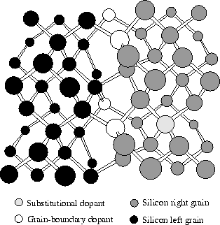
Figure 3.2-4: Three-dimensional perspective drawing of a grain/grain boundary
network. The atoms labeled gb and i refer to substitutional sites of
dopants at the grain boundary and the grain interior, respectively. Dopants
show high possibility to segregate into the grain boundaries where they find
fast diffusion pathes .
These energetically favorable grain boundaries also affect the adjacent grain interior regions. It is possible for dopants to segregate into the grain boundary, if they are close enough and if there is enough space in the grain boundary, which can be already occupied by other dopant atoms. The segregation of dopants into the grain boundary can be described by trapping and emission mechanisms. The capture and emission rates depend on the number of occupied and free states in the grain boundary, where the total number of states is limited by the grain boundary area.
The third transport mechanism is related to the grain growth phenomenon. Due to grain growth, the grain boundaries are moving and so do the dopants incorporated in the grain boundaries. This movement results in a net dopant transport.
As the crystal structure of the polysilicon grain bulk region shows a regular silicon lattice, the diffusion of dopants within the grain interior regions is treated like normal diffusion in silicon (see Section 3.1.4). Additionally, effects like dopant activation and clustering play an important role in the grain bulk and have to be considered for a complete description of the polysilicon diffusion problem.
For practical outdiffusion applications the interface between the
polysilicon and the underlying substrate material plays a major
role. Unfortunately, it is not possible with reasonable effort to fabricate
native-oxide-free poly-/monosilicon interfaces. The thickness and the
chemical properties of this native oxide layer influence the dopant profile
during outdiffusion significantly. By applying moderate diffusion
temperatures, as given by a furnace annealing process (FA), the interface
oxide remains stable and the dopant is able to overcome this diffusion
barrier because of the small extension of this oxide layer ( ![]() ). A
classical dopant segregation approach is used to account for the dopant flux
across the interface (see Section 4.4.2).
Nevertheless, SIMS measurements reveal a typical pile-up in the dopant
concentration on either side of the boundary [Kod92] [Sch85]
, which cannot be explained by segregation kinetics. The interface exhibits
some typical charging capabilities for the dopants. To model the interface
consistently, we assume the interface to be an extraordinary large grain
boundary with fewer free states compared to bulk grain boundaries, because
most of the free sites are already occupied by oxide molecules. This
phenomenon leads to an additional trapping/emission relation for the
interface concentrations (see Section 4.4.3).
). A
classical dopant segregation approach is used to account for the dopant flux
across the interface (see Section 4.4.2).
Nevertheless, SIMS measurements reveal a typical pile-up in the dopant
concentration on either side of the boundary [Kod92] [Sch85]
, which cannot be explained by segregation kinetics. The interface exhibits
some typical charging capabilities for the dopants. To model the interface
consistently, we assume the interface to be an extraordinary large grain
boundary with fewer free states compared to bulk grain boundaries, because
most of the free sites are already occupied by oxide molecules. This
phenomenon leads to an additional trapping/emission relation for the
interface concentrations (see Section 4.4.3).
By increasing the diffusion temperature and the doping concentrations the
native oxide film breaks up and the interface changes its properties. The
typical dopant pile-up vanishes due to dopant transport into the substrate
[Kan94]
. This rupture is not occurring immediately. There is a delay
time ![]() observed from experiments, which is needed to induce the
rupture of the interface native oxide film [Spi93] [Wil92]
. The
delay time depends on the local dopant concentration. Table
(3.2-2) shows a summary of delay times available from literature
for different doping and temperature conditions.
observed from experiments, which is needed to induce the
rupture of the interface native oxide film [Spi93] [Wil92]
. The
delay time depends on the local dopant concentration. Table
(3.2-2) shows a summary of delay times available from literature
for different doping and temperature conditions.
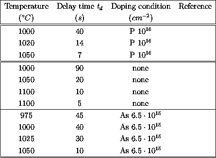
Table 3.2-2: Polysilicon interface break-up delay
time ![]() for different doping conditions and temperatures taken from
literature. There is a significant impact of the doping conditions onto the
delay time.
for different doping conditions and temperatures taken from
literature. There is a significant impact of the doping conditions onto the
delay time.
At temperature above ![]() for doped samples and
for doped samples and ![]() for
undoped samples, epitaxial realignment can occur. The break-up of the
the native oxide is necessary for the onset of epitaxial alignment,
otherwise the temperature must be above
for
undoped samples, epitaxial realignment can occur. The break-up of the
the native oxide is necessary for the onset of epitaxial alignment,
otherwise the temperature must be above ![]() for
recrystallization of a polysilicon layer, which is not an applicable
temperature range for microelectronic processing. The next section gives a
detailed description of the processes occurring during epitaxial realignment
and their influences on the modeling setup.
for
recrystallization of a polysilicon layer, which is not an applicable
temperature range for microelectronic processing. The next section gives a
detailed description of the processes occurring during epitaxial realignment
and their influences on the modeling setup.