To determine feasible lower values of the supply voltage,
a set of tuned CMOS processes was numerically analyzed
by means of process and device simulation. The resulting device
data were used for performance analysis on the circuit
level [61,62].
Both process and device simulation were done using the VISTA
Technology CAD framework to
allow for quick process design and evaluation
[54,55,32].
For the
electrical characterization of the devices MINIMOS [27,69]
was used to calculate a matrix of drain currents
![]() over a range of
over a range of
![]() and
and
![]() for the p-channel and
n-channel transistors. Based on these data, a fast and accurate
table-driven DC analysis of simple gates and inverters is
possible
2.2
[62].
The dynamic behavior was estimated from
capacitance data obtained by AC analysis with MINIMOS.
for the p-channel and
n-channel transistors. Based on these data, a fast and accurate
table-driven DC analysis of simple gates and inverters is
possible
2.2
[62].
The dynamic behavior was estimated from
capacitance data obtained by AC analysis with MINIMOS.
![\includegraphics[scale=0.85]{ulpdop.eps}](img279.gif)
|
| process |
|
|
|
|
|
|
|
|---|---|---|---|---|---|---|---|
| A | 0.2 | 0.067 | -0.059 |
|
|
|
|
| B | 0.5 | 0.260 | -0.240 |
|
|
|
|
| process |
|
|
|
|
|
|
|
|
|---|---|---|---|---|---|---|---|---|
| A | 28 | 23 | 13 | 39 | 0.29ns | 7.2ns | 0.65fJ | 41nW |
| B | 38 | 44 | 31 | 49 | 0.55ns | 1.3 |
4.3fJ | 0.88nW |
The simulated processes were a ![]() process (A) for static
logic and a
process (A) for static
logic and a ![]() process (B) for dynamic logic. The
processes were designed for proper DC characteristics but were not
optimized for speed.
The essential simulation results are compiled in
Tables 2.3 and 2.4.
The device characteristics for process A are
shown in Figs. 2.6 and 2.7.
Figures 2.8 and 2.9
show the inverter transfer curves of both
process A and B.
The noise margins and the inverter delay for both processes
are shown in Figs. 2.10 and 2.11
as functions of the supply voltage, and in
Figs. 2.12 and 2.13 as functions of the
operating temperature.
It can be seen that a ring
oscillator built with process A would work even at
process (B) for dynamic logic. The
processes were designed for proper DC characteristics but were not
optimized for speed.
The essential simulation results are compiled in
Tables 2.3 and 2.4.
The device characteristics for process A are
shown in Figs. 2.6 and 2.7.
Figures 2.8 and 2.9
show the inverter transfer curves of both
process A and B.
The noise margins and the inverter delay for both processes
are shown in Figs. 2.10 and 2.11
as functions of the supply voltage, and in
Figs. 2.12 and 2.13 as functions of the
operating temperature.
It can be seen that a ring
oscillator built with process A would work even at
![]() ,
and by using additional inverters at the gate inputs and outputs one
could also design digital circuits for
,
and by using additional inverters at the gate inputs and outputs one
could also design digital circuits for
![]() ,
but the
overhead of the additional components would be considerable.
,
but the
overhead of the additional components would be considerable.
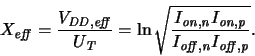
To see how close the two processes are to the absolute lower
limits for
![]() we define the factors
we define the factors
![]() and
and
![]() .
Using (2.11) we get
.
Using (2.11) we get
![]() ,
and we define
,
and we define
From these data one can conclude that the limits for the supply voltage
will be around 200mV for static logic and 500mV for dynamic logic with a
fan-in of 3 at ![]() .
.
![\includegraphics[scale=1.0]{in-stat.eps}](img303.gif)
![\includegraphics[scale=1.0]{out-stat.eps}](img304.gif)
![\includegraphics[scale=1.15]{ix-stat.eps}](img305.gif)
![\includegraphics[scale=1.15]{ix-dyn.eps}](img307.gif)
![\includegraphics[scale=1.0]{nm-02.eps}](img318.gif)
![\includegraphics[scale=1.0]{nm-05.eps}](img319.gif)
![\includegraphics[scale=0.97]{nmtd-t-s.eps}](img320.gif)
![\includegraphics[scale=0.97]{nmtd-t-d.eps}](img321.gif)