The development of the photoresist is modeled as
a surface-controlled etching reaction
[13].
We use Kim's `R'-model to relate the bulk image
to a spatially inhomogeneous etch or development rate
[19].
This development rate is stored on a tensorproductgrid, because the
above discussed differential method requires a
laterally uniform spaced grid to apply the numerically highly efficient
two-dimensional FFT algorithm.
For the simulation of the time-evolution of the development front we have
adapted the recently proposed cellular-based topography
simulator of
[10]
[11]
to read the development rate from the tensorproductgrid.
The basic idea behind this surface advancement algorithm is to apply
a structuring element along the exposed surface which removes
successively photoresist cells
of the underlying cellular geometry representation.
Within the scope of lithography simulation the shape of the structuring
element depends on the precalculated development rate
multiplied by the chosen time step. The principal
operation of the algorithm is illustrated in
Fig. 10.
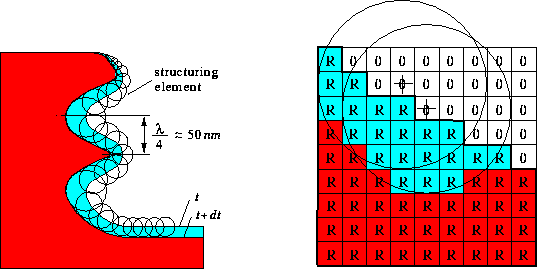
As the development rate
exhibits a strong dependence on the spatial coordinates,
e.g., due to standing waves or notching effects during photoresist exposure,
a sufficiently high number of cells has to be chosen to
resolve these variations.
For example, in case of standing waves we know that the distance between
the maxima and minima of the absorbed light intensity and
therefore also of the development rate is
![]() yielding approximately
yielding approximately
![]() for I-line illumination
(
for I-line illumination
(![]() )
and a refractive index of
)
and a refractive index of
![]() for the photoresist
(c.f. Fig. 10).
For an accurate movement of the development front
the structuring element must not be larger than
this significant distance. In
[10]
and
[11]
it is shown, that the structuring element should be resolved
with approximately 15 cells to avoid rounding and faceting errors.
Hence, at least a cell density of
300 cells/
for the photoresist
(c.f. Fig. 10).
For an accurate movement of the development front
the structuring element must not be larger than
this significant distance. In
[10]
and
[11]
it is shown, that the structuring element should be resolved
with approximately 15 cells to avoid rounding and faceting errors.
Hence, at least a cell density of
300 cells/![]() is needed for photolithographic applications.
The applicability of the structuring element algorithm
for such a cellular geometry resolution has already been demonstrated in
[10]
and
[11].
A further discussion of accuracy issues and rounding effects as
well as a comparision to other surface advancement algorithms
(e.g., string, ray-trace and cell-removal algorithm) can be found in
[20].
is needed for photolithographic applications.
The applicability of the structuring element algorithm
for such a cellular geometry resolution has already been demonstrated in
[10]
and
[11].
A further discussion of accuracy issues and rounding effects as
well as a comparision to other surface advancement algorithms
(e.g., string, ray-trace and cell-removal algorithm) can be found in
[20].